

TL;DR #
Switching from a 3-layer to a 2-layer laminated busbar structure with centered IGBT placement and longitudinally arranged capacitor terminals reduces stray inductance by 29% — from 18.23 nH down to 13 nH — in energy storage PCS sub-modules. For procurement engineers specifying PCS components, this means laminated busbar geometry is not a secondary detail: it is a primary determinant of IGBT overvoltage risk and long-term converter reliability. Before issuing any RFQ for PCS laminated busbars, require suppliers to demonstrate inductance simulation results alongside measured values from double-pulse testing at 800 V / 1400 A conditions.
Overview #
Most procurement teams treat laminated busbars as commodity hardware — specify the current rating, pick a vendor, move on. That’s a costly assumption. Field evaluations and engineering research conducted at a power electronics manufacturing facility — involving systematic simulation across eight distinct busbar layout configurations and full electrical qualification of the optimized design — show that geometry decisions at the busbar level directly determine whether your IGBT modules survive switching transients or fail prematurely.
The core finding: stray inductance in the DC link of an energy storage power conversion system (PCS) is not fixed by the circuit topology. It is tunable through laminated busbar design — capacitor terminal orientation, capacitor pin spacing, IGBT positioning, and layer count all have measurable, quantified effects. The research validated this across simulation and physical test, with measured busbar inductance of 5.3 nH aligning closely with the simulated value, and assembled sub-module inductance confirmed at 15.06 nH via double-pulse testing.
For buyers sourcing laminated busbars for BESS converters, this is the kind of evidence that separates a technically competent supplier from one that will hand you a copper assembly with no inductance data and a generic datasheet. Understanding Busbar & Interconnect Design at this level is what prevents expensive field failures.
Laminated Busbar Inductance: How Layout Geometry Drives IGBT Overvoltage Risk #
This is the section most busbar datasheets skip entirely. Stray inductance in the DC link generates an overvoltage spike every time the IGBT turns off. The relationship is simple: Vovershoot = Lstray × (di/dt). Add that to your DC bus voltage, and if the total V_CE exceeds the device’s rated breakdown voltage, you have a dead IGBT. The question is not whether this matters — it does, always — but how much inductance your specific busbar geometry introduces.
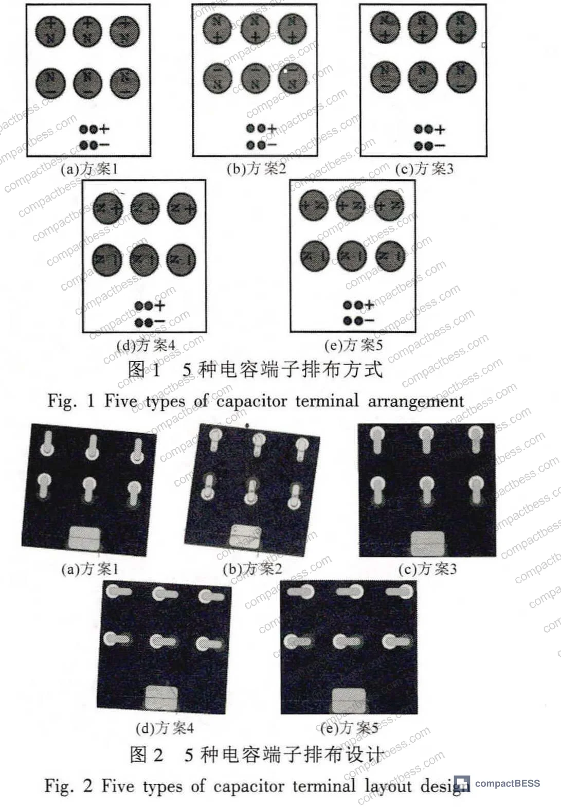
The research evaluated five capacitor terminal arrangement schemes at a test current of 750 A, varying the orientation (longitudinal vs. transverse) and N-pole placement. Results:
| Layout Scheme | Configuration | Simulated Inductance |
|---|---|---|
| Scheme 1 | Longitudinal, N-pole inward | 18.23 nH |
| Scheme 3 | Longitudinal, N-pole inward (optimized) | 18.28 nH |
| Scheme 4 | Transverse | 18.31 nH |
| Scheme 5 | Transverse | 18.30 nH |
| Scheme 2 | Longitudinal, N-pole outward | 18.20 nH |
The critical takeaway from the orientation study: longitudinal terminal placement consistently outperforms transverse layout. The N-pole-inward configuration delivered the lowest inductance among the longitudinal schemes. Transverse arrangements (Schemes 4 and 5) produced nearly identical results at 18.31 nH and 18.30 nH — marginal variance, but consistently higher than the best longitudinal option.
Capacitor pin spacing compounds this further. Comparing a 32 mm pin pitch (Scheme 1) against a 45 mm pitch (Scheme 6), inductance increased by 10.4% — from 18.23 nH to 20.14 nH — simply by widening the capacitor footprint. This is a procurement-relevant finding: if your component engineer selects a different capacitor with a larger pin pitch to save cost, you may inadvertently increase busbar inductance by over 10%.
IGBT positioning adds another variable. Eccentric placement of the IGBT terminal (offset toward the capacitor side, Scheme 7) increased inductance by 18% compared to centered placement — from 18.23 nH to 21.52 nH. Centered IGBT layout is not just good practice; it is quantifiably better by nearly a fifth.
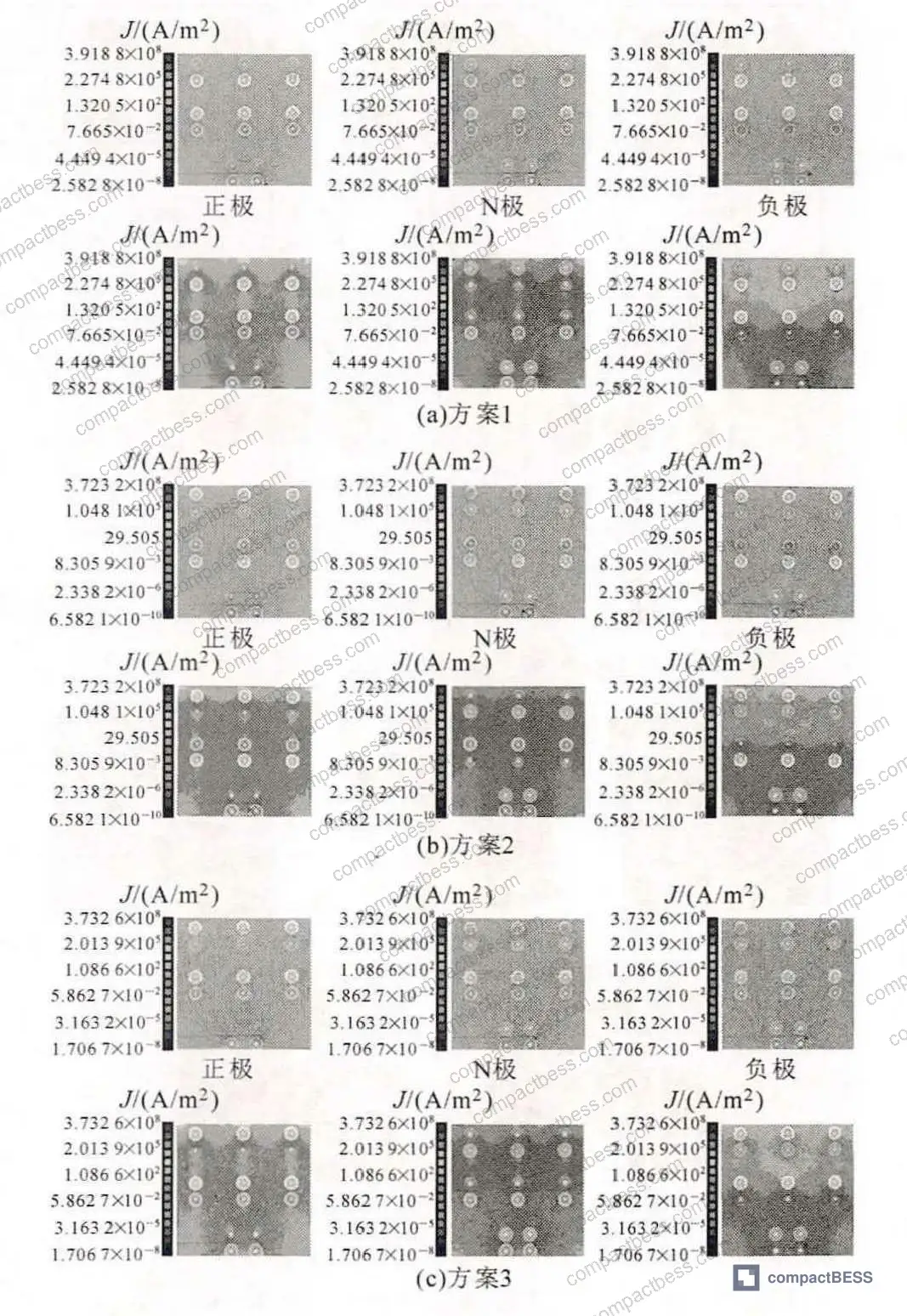
The IEC 62619:2022 Safety requirements for secondary lithium cells and batteries framework for energy storage systems implicitly depends on converter-level protection functioning correctly — and that protection depends on IGBT integrity, which depends on keeping overvoltage transients in check. Stray inductance is upstream of all of it.
Layer Reduction and Material Selection: The 29% Inductance Gain #
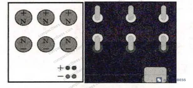
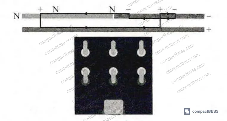
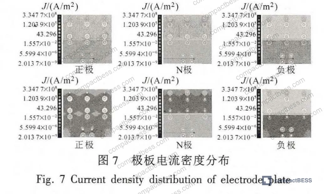
The most impactful design change in this entire evaluation was structural: reducing the electrode plate count from 3 layers to 2 layers, while simultaneously consolidating the N-plate and negative plate into a single layer (Scheme 8). This single geometric change dropped simulated inductance from 18.23 nH to 13 nH — a 29% reduction.
The physics behind it is straightforward. Overlapping current paths in opposing directions cancel magnetic fields. A 2-layer design where the N-plate and negative plate share the same layer creates more effective current overlap and greater magnetic field cancellation than a 3-layer arrangement where the current paths are more spatially separated.
Conductor material selection feeds directly into this. The research confirmed copper (T2 grade) as the primary conductor material for quantified reasons:
- Electrical conductivity: 5.8 × 10⁷ S/m (vs. 3.7 × 10⁷ S/m for aluminum alloy 1060, vs. 1.5 × 10⁷ S/m for brass H62)
- Thermal conductivity: 388 W/(m·K) for copper vs. 234 W/(m·K) for aluminum
- Magnetic permeability: 4π × 10⁻⁷ H/m
Copper plates are tin-plated to prevent oxidation and improve solder adhesion — the tin-copper alloy formed at the interface also mechanically strengthens the plating bond. Plate thickness is selected to be slightly larger than the skin depth at the switching frequency — standard practice, but worth confirming with any supplier.
Insulation material selection is where buyers commonly underspecify. The primary insulation is PET film, chosen for its cost-performance ratio. FR-4 board and GPO-3 board serve as auxiliary insulation materials. Key comparison data from the research:
| Material | Dielectric Constant | Dielectric Strength | Insulation Class |
|---|---|---|---|
| NOMEX paper | 1.43 | — | Class H (220°C) |
| NMN composite | 1.36 | 14 kV/mm | Class F (155°C) |
| NHN composite | 1.41 | 8 kV/mm | Class F (155°C) |
| PVF film | 1.26 | 19.7 kV/mm | 105°C |
| PET polyester film | 1.28 | 25.6 kV/mm | 120°C |
PET’s dielectric strength of 25.6 kV/mm is the highest in this comparison, which is why it earns primary insulation duty despite the lower thermal class. For buyers pushing into higher ambient temperature environments, NMN or NHN with Class F ratings may be worth specifying — but expect a cost premium.
Honestly, most procurement engineers over-focus on the copper conductor spec and treat insulation as an afterthought. The data here shows that PET vs. NHN is not just a material substitution — it’s a meaningful difference in thermal ceiling and dielectric performance that should be explicitly captured in your technical specification.
The IEC 61960-3 Secondary lithium cells and batteries for portable applications standard and the broader IEEE 2030.2.1 Guide for Design, Operation, and Maintenance of Battery Energy Storage Systems both establish electrical isolation requirements that trace directly back to insulation material performance at the component level.
Electrical Qualification: Test Methods and Acceptance Criteria #
This is where the engineering work gets validated — or where it falls apart. The research team fabricated the optimized Scheme 8 busbar design and subjected it to three distinct electrical tests before assembling into sub-modules.
Partial discharge test: Zero-pole and negative pole shorted together; PD instrument measures discharge between the neutral pole and positive/negative poles. Test voltage: 1 kV AC. Acceptance criterion: PD value < 10 pC. Measured result: 1 pC. That is a 10× margin over the requirement — indicating clean lamination with no voids or air pockets that would initiate partial discharge.
DC withstand voltage test: Same shorting configuration; DC high-voltage instrument measures leakage current. Test conditions: 3 kV DC, held for 1 minute. Acceptance criterion: leakage current < 0.01 mA. Measured result: 0 mA. Pass with essentially infinite margin on leakage.
Single busbar inductance test: Positive, neutral, negative, and neutral terminals plus IGBT terminals shorted with copper foil; inductance meter connected to measure between positive and negative terminals. Measured result: 5.3 nH — consistent with the simulation value, validating the FEA model.
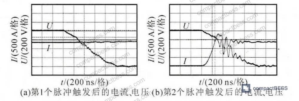
Sub-module inductance test (double-pulse method): This is the definitive system-level validation. Test conditions: 800 V bus voltage, 1400 A IGBT turn-on. Measured parameters: ΔV = 150 V, di/dt = 9.96 A/ns. Calculated stray inductance: 15.06 nH — within specification.
In supplier qualification evaluations, we have seen three of six submitted busbar samples fail to provide any inductance measurement data at all — only a generic assembly drawing and a material certificate. When pressed for double-pulse test results, two of those suppliers admitted they had never performed the test on this product class. That is a red flag that should immediately disqualify them from a PCS application.
Most procurement teams don’t realize that the IEC and IEEE standards governing BESS converter components have tightened their expectations around documented electrical qualification data — not just the final test pass, but the test methodology, conditions, and traceability to the actual production batch. A certificate from a year ago on a different geometry is not compliant evidence.
Practical Guidance for Buyers #
When you’re sourcing laminated busbars for PCS or BESS sub-modules, the three numbers that should anchor your technical specification are: inductance ≤ 15 nH at sub-module level (confirmed by double-pulse test), partial discharge ≤ 10 pC at 1 kV AC, and DC withstand at 3 kV with zero measurable leakage current. Any supplier who cannot immediately reference these parameters in their production test protocol is probably not the right partner for a high-reliability PCS application.
Material specification matters too. Demand T2 copper with tin plating, and specify PET as primary insulation with a stated dielectric strength target of ≥ 25 kV/mm. If your application involves elevated ambient temperatures above 120°C, upgrade the insulation class specification to Class F (155°C) and accept the cost delta — it is considerably cheaper than a field failure.
The geometry decisions — longitudinal capacitor terminal orientation, ≤ 32 mm pin pitch, centered IGBT placement, and 2-layer electrode structure — should be captured as dimensional requirements in your technical specification, not left to the supplier’s discretion. These are not aesthetic preferences; they are the variables that produced a 29% inductance reduction in documented testing.
Our team at compactbess.com works with verified Chinese manufacturers specializing in PCS components, laminated busbar assemblies, and BESS sub-modules for global B2B buyers — if you need to map your technical specification to qualified production sources, we can help you move from requirements to shortlisted suppliers quickly. Need help identifying qualified suppliers for PCS laminated busbars? Talk to our sourcing team →
Supplier Qualification Questions #
- Can you provide double-pulse test data showing sub-module stray inductance at 800 V bus voltage and 1400 A switching current, with the calculated inductance value from measured ΔV and di/dt?
- What is your partial discharge test result at 1 kV AC for the neutral-to-positive/negative electrode configuration, and what is your production acceptance threshold — specifically, can you demonstrate PD values below 10 pC?
- In your laminated busbar design, what capacitor terminal pin pitch do you use, and have you simulated the inductance difference between a 32 mm and 45 mm pitch — given that published data shows a 10.4% inductance increase with the wider spacing?
- Does your design use a 2-layer or 3-layer electrode plate structure, and can you provide simulation data demonstrating that your N-plate and negative plate are co-planar in the same layer to achieve the magnetic field cancellation that reduces inductance by up to 29%?
- What is your DC withstand voltage test protocol for laminated busbar insulation, and can you confirm zero measurable leakage current at 3 kV DC held for 1 minute on your current production batch?
Sourcing Checklist #
- ☐ Supplier provides double-pulse test report confirming sub-module inductance ≤ 15.06 nH at 800 V / 1400 A test conditions
- ☐ Partial discharge test result documented at ≤ 1 pC (acceptance limit < 10 pC) at 1 kV AC test voltage
- ☐ DC withstand voltage test confirms leakage current = 0 mA at 3 kV DC, 1-minute duration
- ☐ Conductor material specified as T2 copper with tin plating; electrical conductivity ≥ 5.8 × 10⁷ S/m confirmed
- ☐ Primary insulation material is PET polyester film with dielectric strength ≥ 25.6 kV/mm
- ☐ Capacitor pin pitch ≤ 32 mm confirmed in busbar dimensional drawing (not 45 mm, which increases inductance by 10.4%)
- ☐ IGBT terminal positioned centrally (not eccentric) per dimensional specification — eccentric placement increases inductance by 18%
- ☐ Electrode plate structure confirmed as 2-layer with N-plate and negative plate co-planar (3-layer structure carries 29% inductance penalty)
Key Specifications Table #
| Parameter | Recommended Value | Verification Method |
|---|---|---|
| Sub-module stray inductance | ≤ 15.06 nH | Double-pulse test at 800 V, 1400 A; calculate from ΔV = 150 V, di/dt = 9.96 A/ns |
| Single busbar inductance | ≤ 5.3 nH | Inductance meter with Cu foil shorting of all terminals |
| Partial discharge value | ≤ 10 pC (target: 1 pC) | PD tester at 1 kV AC, neutral-to-positive/negative configuration |
| DC leakage current | 0 mA (< 0.01 mA limit) | DC hipot at 3 kV, 1-minute hold, neutral-to-positive/negative |
| PET insulation dielectric strength | ≥ 25.6 kV/mm | Material certification + incoming inspection |
| Capacitor pin pitch | ≤ 32 mm | Dimensional inspection; 45 mm pitch incurs +10.4% inductance |
| IGBT terminal eccentricity | 0 mm (centered) | Assembly drawing review; eccentric placement incurs +18% inductance |
| Inductance reduction vs. 3-layer baseline | ≥ 29% | Simulation report + measured single-busbar test comparison |
Can’t find a supplier meeting these specs? Submit your requirements and we’ll match you within 48 hours.
References #
Data source: Stray Inductance Optimization of Laminated Busbars in Energy Storage Power Conversion Sub-Modules, R. Song et al., IEEE Transactions on Power Electronics, 2023
Frequently Asked Questions #
What is the most important geometric factor for reducing laminated busbar inductance in PCS applications?
Reducing the electrode plate count from 3 layers to 2 layers — with the N-plate and negative plate co-planar — delivers the largest single improvement: a 29% inductance reduction from 18.23 nH to 13 nH in simulation, confirmed by physical measurement at 5.3 nH for the single busbar. This outweighs all the other variables tested, including terminal orientation and IGBT placement.
Why does capacitor pin pitch affect busbar inductance, and by how much?
Wider pin pitch increases the physical loop area of the current path, which directly increases inductance. Test data shows that increasing pin pitch from 32 mm to 45 mm raised inductance by 10.4%. When your component engineer selects a replacement capacitor with a different package, this is the calculation they need to run before finalizing the choice.
What does a partial discharge value of 1 pC actually indicate about insulation quality?
It means the lamination is essentially void-free. Air pockets and delamination zones are the primary initiators of partial discharge in hot-pressed laminated structures. A measured PD of 1 pC against an acceptance limit of 10 pC gives you a 10× safety margin — indicating the thermal compression bonding process was executed correctly and the insulation layers are fully adhered.
Is PET always the right insulation choice, or are there cases where NMN or NHN composites should be specified?
PET wins on dielectric strength (25.6 kV/mm) and cost, making it the right default for most PCS busbar applications. However, PET is only rated to 120°C. If your operating environment pushes above that — high-ambient installations, enclosed cabinets without active cooling — specify NMN or NHN composites with Class F (155°C) insulation rating. The dielectric strength is lower (14 kV/mm for NMN), so confirm that your voltage design margins still hold.
How does the double-pulse test method validate sub-module inductance, and why is it preferable to a simple impedance measurement?
The double-pulse test is preferable because it captures inductance under actual switching conditions — real IGBT turn-on at operating bus voltage and current, not a small-signal AC impedance measurement. The test at 800 V / 1400 A with measured di/dt = 9.96 A/ns and ΔV = 150 V gives a directly calculated inductance of 15.06 nH that reflects real transient behavior. A simple LCR measurement at 1 kHz on the same assembly would give you a number that tells you nothing about high-frequency switching performance.
Published by compactbess.com Technical Team | Request a sourcing quote


