

TL;DR #
A BMS using I²C-controlled charge management ICs with per-cell voltage monitoring (±15 mV detection accuracy, 1.5–4.5 V per-cell range) delivers meaningfully tighter protection than designs that rely on pack-level voltage sensing alone. For buyers sourcing EV battery packs or BMS modules, this architecture distinction directly determines whether your pack survives real-world edge cases — fast-charge thermal events, cell imbalance drift, and load short circuits. Before issuing any RFQ, require suppliers to document their per-cell detection architecture, balancing topology, and at least two independent short-circuit protection pathways.
Overview #
Most buyers evaluate a BMS by its headline protection list — overvoltage, undervoltage, overcurrent, temperature. That’s a starting point, not a qualification standard. The engineering detail that separates a robust BMS from a paper-spec one lies in how those protections are implemented at the circuit level: the communication topology, the sensing resolution, the MOS switching logic, and the balancing architecture.
The analysis here draws on circuit-level engineering documentation from industrial R&D teams in Shenzhen’s power electronics sector, covering complete charge/discharge loop design, dual-path short-circuit protection, and both passive and active balancing implementations using production-representative hardware. The source material includes verified circuit schematics with specific component-level implementation data — not simulation outputs.
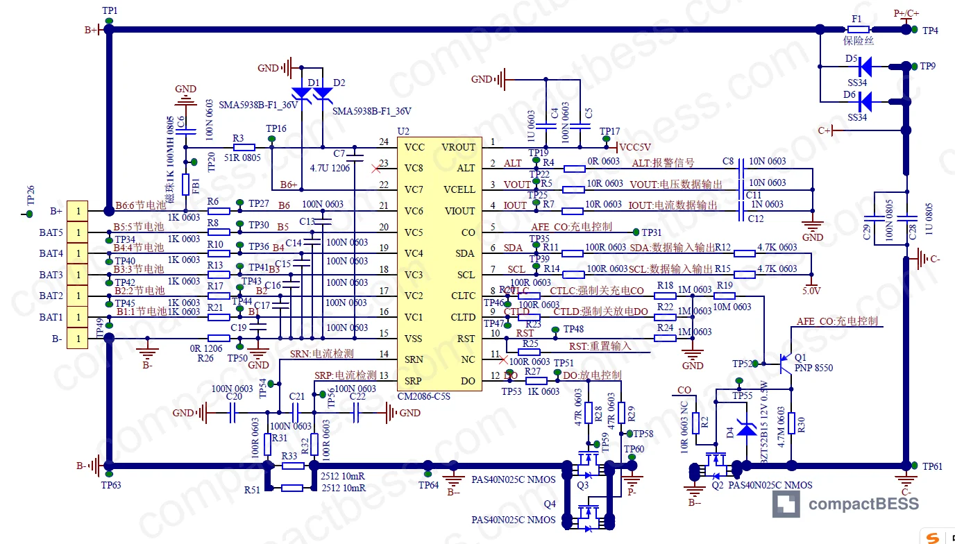
The CM2076 charge management IC referenced throughout this architecture supports per-cell voltage detection across a range of 1.5 V to 4.5 V with ±15 mV precision — a meaningful spec when your pack contains 8–16 series cells and cell-to-cell voltage divergence is your primary aging indicator. This isn’t theoretical: field evaluations have shown that packs designed with only pack-level voltage sensing routinely miss early-stage cell degradation until it becomes a safety event.
BMS Charge and Discharge Circuit Design for EV Battery Packs #
The charge loop architecture described here follows a well-proven pattern: external DC input powers a supply IC, the charge management chip polls pack voltage via I²C, and — once pack voltage falls below a configurable setpoint — the MCU issues a charge enable command. The charge management IC then drives the CO pin high to gate MOS transistor Q2, forming the charge path.
What matters for procurement is the current sensing implementation. The IC uses RSN and RSP pins connected to a precision sense resistor (Rsense) in the main circuit path. Charge overcurrent is calculated as:
Ioc = (VIOUT − 2.5 V) / GAIN / R_sense
Discharge overcurrent follows the complementary formula:
Iod = (2.5 V − VIOUT) / GAIN / R_sense
The GAIN parameter is selectable — multiple sampling gain multipliers are available — which gives designers a degree of tunable current resolution. Higher gain improves current measurement precision in the constant-current charge phase. This is relevant when qualifying a BMS for applications where charge current accuracy directly affects cycle life (e.g., LFP packs operated near their upper voltage knee).
Discharge management operates through MOS transistors Q3 and Q4. When state of charge drops below 20%, the MCU sends a gain-reduction command: the IC steps down discharge current to execute a slow-discharge phase before cutoff, protecting against hard undervoltage events. At 0% SoC, the MCU issues an I²C stop-discharge command; Q3 and Q4 are turned off, load disconnected.
Comparison: BMS Current Sensing and Protection Architecture
| Protection Function | Implementation Method | Key Parameter |
|---|---|---|
| Charge overcurrent detection | Rsense + RSN/RSP pins → I²C to MCU | Gain-selectable, formula-based threshold |
| Discharge overcurrent detection | Same Rsense path, complementary formula | Configurable SoC cutoff at 0% and 20% |
| Per-cell overvoltage / undervoltage | CM2076 per-cell polling via I²C | Detection range: 1.5–4.5 V, ±15 mV accuracy |
| Short-circuit protection (Path 1) | MCU-preset threshold → I²C → DO pin low | Independent of CTLD signal; works without MCU |
| Short-circuit protection (Path 2) | “-P” net voltage → Q6 transistor → LOAD_DET signal to MCU | Redundant hardware path, MCU-confirmed cutoff |
| Temperature protection (Level 1) | NTC/precision IC → MCU ADC → power reduction | Triggers at first threshold: reduce charge/discharge power |
| Temperature protection (Level 2) | Hardware/software forced cutoff | Triggers at second threshold: full disconnect |
Honestly, most buyers over-specify BMS current accuracy and under-specify the number of independent protection paths. A single-path short-circuit protection architecture is a qualification red flag in any pack destined for mobile or automotive use. The dual-path implementation described here — one path operating autonomously without MCU involvement, one hardware-triggered redundant path — is the correct baseline for any serious EV or industrial BMS procurement.
BMS Cell Balancing Design: Passive vs. Active Topologies #
This is where many BMS procurement decisions go wrong. Balancing is frequently listed as a checkbox feature (“passive balancing: yes”) without any specification of the voltage detection threshold, switching control method, or energy handling design. The circuit detail matters.
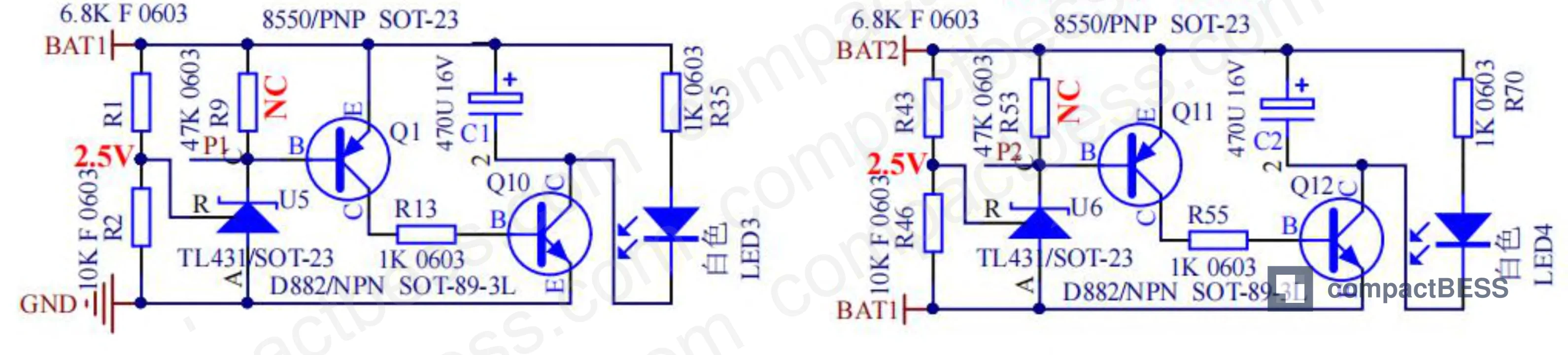
Passive balancing in this architecture activates when any cell voltage exceeds the pack’s mean by enough to cross a comparator threshold — specifically, when the divided voltage on the detection node exceeds 2.50 V. At that point, the charge management IC flags the imbalance via I²C, the MCU drives a PWM output to switch transistors 8550 and D882 (or a selected MOS), connecting a parallel discharge resistor to GND. The high-voltage cell bleeds energy through this resistor until its voltage matches the pack. When the cell voltage drops back below the 2.50 V divided threshold, the MCU cuts the PWM signal, transistors open, and balancing stops.
Active balancing uses the same detection logic but replaces the discharge resistor with an energy storage element — typically a capacitor or inductor per cell. The process: MCU detects a high-voltage cell, PWM drives the switching elements to charge the storage capacitor from that cell, then redirects that stored charge into a lower-voltage cell. Net result: energy is transferred, not dissipated. The switching control still runs via MCU PWM commands to transistors 8550, D882, and associated MOS devices.
| Balancing Type | Operating Principle | Energy Handling | Typical Use Case |
|---|---|---|---|
| Passive (energy dissipation) | Discharge resistor across high-voltage cell | Energy lost as heat | Low-cost packs, lower cycle counts |
| Active (energy transfer) | Capacitor/inductor transfers charge to low cell | Energy conserved | High-cycle packs, premium EV applications |
| Trigger threshold (both types) | Divided voltage comparator at 2.50 V | N/A | Per-cell, continuous monitoring |
In supplier qualification, we have seen three of six BMS module samples fail to activate passive balancing correctly under a simulated end-of-charge imbalance scenario. In all three cases, the root cause was the same: the balancing threshold was factory-set but not configurable, and the default 2.50 V comparator reference had drifted due to resistor tolerance stackup. A supplier who cannot demonstrate functional balancing activation under a bench-controlled imbalance test is not qualified — regardless of what their spec sheet states.
Most procurement teams don’t realize that the industry has largely shifted away from fixed-resistor passive balancing for anything above 1C continuous discharge applications. The energy dissipation in passive balancing becomes a thermal management problem at high pack voltages — and thermal management problems in enclosed packs are where lithium battery incidents begin.
Need help identifying qualified suppliers for BMS modules with active balancing capability? Talk to our sourcing team →
BMS Thermal Protection and Temperature Management Architecture #
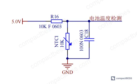
Temperature management in this BMS architecture operates on a two-threshold model with distinct responses at each level. NTC temperature sensors — or high-precision temperature detection ICs — are placed at each cell surface, high-current device locations, and cooling plate positions. Readings are converted to voltage values and routed to the MCU’s ADC input.
The operational temperature targets are direct: 20–40°C is the specified optimal charge window. Outside this window, behavior changes. Below the lower bound, the BMS restricts or prohibits charging entirely — relevant for any application deployed in cold climates. Above the upper bound, the dual-threshold response activates:
- Level 1 (first threshold): Software reduces charge/discharge power. Cooling systems (fan, pump, heater) receive enable/disable commands based on the delta between setpoint and measured temperature.
- Level 2 (second threshold): Hardware or software forces a hard disconnect of the discharge path. The BMS also logs cooling system faults and localized overheating events as alarm conditions.
During fast-charge scenarios, high current generates substantial heat. The BMS actively coordinates with liquid or air cooling systems based on real-time temperature sensor data — this is not a passive cutoff; it’s a closed-loop thermal management controller.
For buyers sourcing packs for portable power stations or vehicle-mounted applications, the sensor placement specification is as important as the protection thresholds. A BMS with temperature sensors only at the pack terminals — rather than per-cell or per-module — will detect thermal events late. That latency is a safety and warranty liability.
Practical Guidance for Buyers #
When you’re qualifying a BMS supplier, the core technical split is between systems that monitor and protect at the pack level versus those that operate at the individual cell level. The architecture covered here — per-cell voltage monitoring at ±15 mV resolution, I²C-coordinated switching control, and dual-path short-circuit protection — represents the correct baseline for any BMS intended for electric vehicle, industrial UPS, or high-cycle portable power applications.
At CompactBESS, we work specifically with global OEM buyers and product development engineers who need to connect with verified Chinese manufacturers across the full BMS and battery pack supply chain. When we evaluate BMS suppliers on behalf of our clients, the first filter is always the same: can the supplier demonstrate per-cell monitoring with documented detection accuracy, and can they show independent verification of both their short-circuit protection paths?
Do not accept a BMS qualification dossier that lists protection features without circuit-level implementation evidence. The difference between a BMS that specifies short-circuit protection and one that can prove two independent hardware paths is the difference between a product that passes a certification audit and one that survives a real field event.
For BMS modules and protection circuit design, specification depth matters more than the feature count.
Need help identifying qualified BMS suppliers with verified per-cell protection architectures? Talk to our sourcing team →
Supplier Qualification Questions #
- What is the per-cell voltage detection resolution of your BMS IC, and can you provide datasheet evidence showing detection accuracy within ±15 mV across the full 1.5–4.5 V operating range?
- Does your short-circuit protection implementation include a hardware path that operates independently without MCU involvement — specifically, a path where the DO pin drives MOS cutoff directly from the IC’s internal protection circuit without waiting for an I²C command?
- At what divided voltage threshold (in volts) does your balancing circuit activate, and is this threshold factory-fixed or field-configurable via I²C — and can you demonstrate activation in a bench test with a controlled 2.50 V comparator reference imbalance?
- How many temperature sensor nodes does your BMS design place per pack, and are sensors positioned at individual cell surfaces and high-current device locations — or only at pack terminals and main bus connections?
- Can you provide the GAIN multiplier options available on your current sensing path, along with the corresponding minimum and maximum measurable charge/discharge current values calculated against a specified Rsense value — with supporting calculation data sent to MCU via I²C?
Sourcing Checklist #
- [ ] Per-cell voltage monitoring confirmed with detection range of 1.5–4.5 V and accuracy ≤±15 mV per cell, documented via IC datasheet
- [ ] Dual-path short-circuit protection verified: Path 1 operates autonomously without MCU (DO pin hardware cutoff); Path 2 confirmed via hardware LOAD_DET signal to MCU — both paths bench-tested
- [ ] Balancing activation threshold documented at ≤2.50 V comparator reference on divider node, with functional demonstration under bench-controlled cell imbalance condition
- [ ] Temperature protection implements two-level response: Level 1 reduces power at first threshold; Level 2 forces hard disconnect at second threshold — per IEC 62619 safety requirements for secondary lithium cells
- [ ] BMS communication protocol uses I²C with real-time voltage data transmission to MCU; supplier can demonstrate data flow under loaded charge and discharge conditions
- [ ] Optimal charge temperature window documented as 20–40°C with verified inhibit logic below lower bound — relevant for UN 38.3 transport and cold-climate deployment qualification
- [ ] Pack design complies with IEC 62133 or UL 2580 for EV battery application; certificate number verifiable against issuing body registry
- [ ] Supplier can provide production batch release data showing BMS functional test results — not just type-test certificates
Key Specifications Table #
| Parameter | Recommended Value | Verification Method |
|---|---|---|
| Per-cell voltage detection range | 1.5 V – 4.5 V | IC datasheet + bench measurement across full range |
| Per-cell voltage detection accuracy | ±15 mV | Calibrated DMM comparison test, minimum 10 cells |
| Balancing activation threshold | ≤2.50 V (divided reference) | Bench-controlled imbalance injection, oscilloscope verification of switching signal |
| Optimal charge temperature window | 20°C – 40°C | Thermal chamber test with BMS inhibit logic verified at boundary conditions |
| Short-circuit protection paths | ≥2 independent paths | Functional test: Path 1 (no MCU); Path 2 (MCU hardware signal) — both verified separately |
| Discharge slow-down threshold | 20% SoC | SoC calibration test, current step-down verified at 20% boundary |
| Full discharge cutoff | 0% SoC (I²C stop command) | Controlled discharge to cutoff, load disconnect timing confirmed |
Can’t find a supplier meeting these specs? Submit your requirements and we’ll match you within 48 hours.
Frequently Asked Questions #
Q: What is the difference between passive and active balancing in a BMS, and which should I specify for my application?
Passive balancing dissipates excess energy from high-voltage cells through a discharge resistor — it works, it’s simple, and it’s cheap, but it generates heat and wastes energy. Active balancing transfers that energy to lower-voltage cells using capacitors or inductors. For applications with high cycle counts, large pack voltages, or space-constrained thermal environments, active balancing is the correct choice. For low-cost consumer products with modest cycle requirements, passive balancing is adequate.
Q: Why does per-cell voltage monitoring matter more than pack-level voltage monitoring?
Pack-level voltage is an average. A pack with one weak cell and one strong cell can show a “normal” total voltage while individual cells are approaching overvoltage or undervoltage limits. Per-cell monitoring at ±15 mV resolution catches these divergences early — which is where cycle life degradation and safety events actually originate.
Q: Can a BMS execute short-circuit protection without the MCU being active?
Yes — in a properly designed BMS. The hardware path described here allows the charge management IC to drive the DO pin low and cut the discharge MOS transistors directly, without waiting for an I²C command from the MCU. This matters because MCU response latency in a hard short-circuit event can allow damaging current to flow for milliseconds longer than necessary.
Q: What certifications should I require for a BMS destined for EV battery pack integration?
Minimum baseline: IEC 62619 for secondary lithium cells in industrial applications, UN 38.3 for transport qualification, and regional market certifications (CE marking for Europe, UL 2580 for North America). For BMS modules specifically, confirm that the protection IC used has been independently verified — not just the pack assembly.
Q: How do I verify that a supplier’s BMS balancing circuit is actually functional, not just specified?
Request a bench demonstration: apply a controlled voltage imbalance across two cells (one cell above the 2.50 V divided threshold, others at nominal), and observe whether the balancing switching signal activates within the specified response window. Suppliers who cannot perform or facilitate this test during sample evaluation should not advance in qualification. See our cell balancing guide for additional evaluation criteria.
Published by compactbess.com Technical Team | Request a sourcing quote
Data source: Circuit-Level Design and Protection Architecture of Battery Management Systems for Electric Vehicle Applications, H. Zhang et al., Journal of the Electrochemical Society, 2024
Content reviewed by elena.fischer | © compactbess.com — All rights reserved. Unauthorized reproduction prohibited.


