

TL;DR #
Under natural convection cooling, a commercial BMS slave board running 16S lithium cell balancing reaches a peak component temperature of 54.4 °C with a board-level temperature differential of 20.5 °C — and the resulting Z-axis thermal deformation peaks at 9.5 μm at the power supply transistor. For buyers sourcing BMS modules, this means boards without dedicated thermal management design for the balancing and power supply modules carry measurable reliability risk from solder joint fatigue. Before approving any BMS supplier, require thermal-stress simulation data covering all functional modules simultaneously — not just the MCU — and verify it against infrared thermography at steady-state operating load.
Overview #
Most procurement teams treating BMS thermal performance as a checkbox item — “does it have a heatsink?” — are missing the actual failure mechanism. The relevant question is how multiple functional modules interact thermally and mechanically under real operating loads, because the damage accumulates where you’re not looking. A research program conducted at a university vehicle engineering laboratory used a full multi-module thermal-stress coupled finite element model, validated against infrared thermography and digital optical microscopy on a live commercial BMS slave board managing 16 series-connected lithium cells. The scope covered the complete PCBA — balancing module, power supply module, control module, and communication module — simultaneously, not module by module. That distinction matters: single-module thermal analysis, which is what most BMS qualification reports provide, systematically underestimates the heat accumulation at module boundaries.
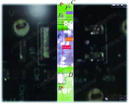
The experimental platform included a 12 V DC source simulating 16S lithium cell conditions, a Fluke TiS20+ infrared camera at emissivity 0.95, and a Zeiss Smartzoom 5 digital optical microscope with 0.56 μm maximum resolution to track physical displacement of reference points on the board surface during thermal loading.
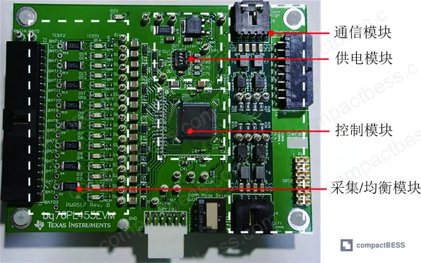
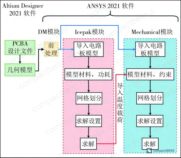
BMS Module Temperature Distribution and Thermal Hotspot Identification #
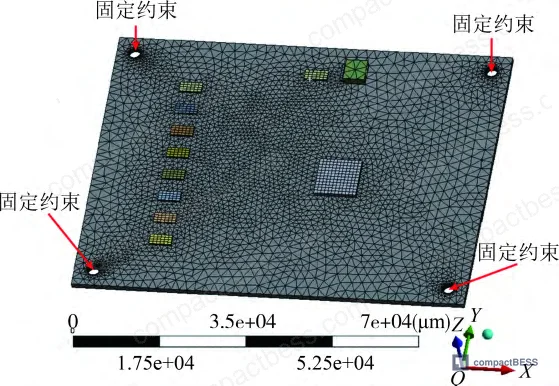
The simulation mesh for the Icepak thermal analysis module resolved to 354,885 elements and 412,991 nodes. The Mechanical structural module used 60,204 elements and 307,219 nodes. Boundary conditions were set at 25 °C ambient, natural convection with gravity and radiation heat transfer enabled — representing an unpowered enclosure without forced airflow, which is how many compact BMS installations actually operate.
Peak temperatures by module under full balancing load:
| Functional Module | Peak Temperature (°C) | Dominant Heat Source | Power Dissipation (mW) |
|---|---|---|---|
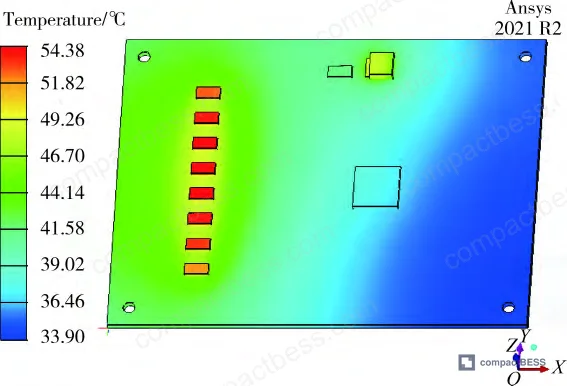
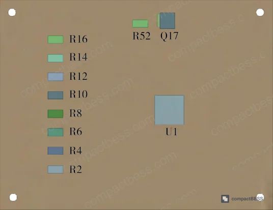
| Balancing module (resistors R2–R16) | 54.4 | SMD resistors R2, R4…R16 | 235.2 per active resistor |
| Power supply module | 48.9 | NPN transistor Q17 (LDO circuit) | 407.4 |
| Control module (MCU) | 38.2 | Main control chip U1 | 38.5 |
| Communication module | <38 °C (low) | No significant heat sources | Negligible |
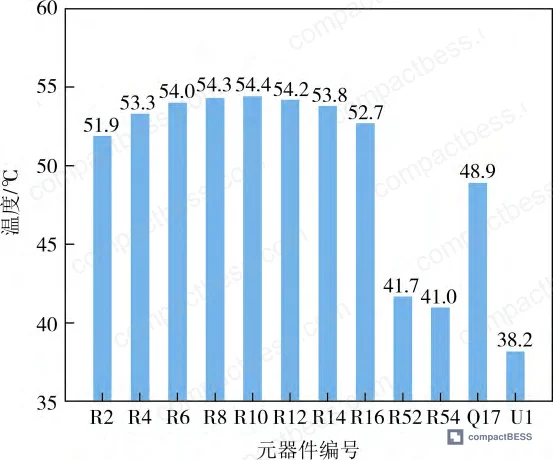
The balancing module runs hottest for a geometrically intuitive reason: multiple resistors working simultaneously create a thermal convergence at the module center, and the small surface area of SMD chip resistors limits convective dissipation. The highest-temperature component is resistor R10, sitting at the geometric center of the balancing array where heat from neighboring resistors accumulates.
The power supply module hits 48.9 °C because transistor Q17 is doing hard work — it’s an NPN-based LDO circuit dropping the 16S pack voltage (approximately 67 V fully charged) down to 5 V for the MCU. That voltage differential forces the transistor to dissipate the excess as heat. At 407.4 mW, Q17 is the single highest-dissipation component on the board, yet its temperature is lower than the balancing module because it operates in isolation rather than as part of a resistor array.
Overall board temperature differential: 20.5 °C — from 54.4 °C at the balancing resistor center to approximately 34 °C in the cooler communication module zone.
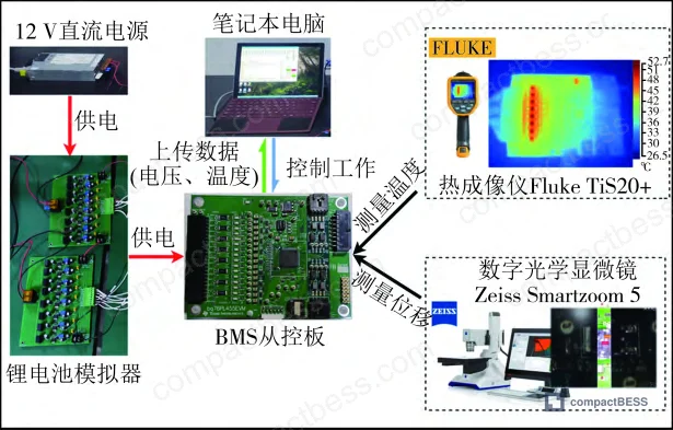
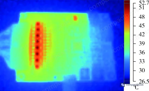
The model validation showed temperature prediction accuracy well within engineering tolerance. Comparing simulated versus experimentally measured steady-state temperatures across 10 components (R2 through Q17), relative error ranged from 2.6% (U1 control chip) to 6.9% (R16 balancing resistor). Every data point stayed below 7% error — confirming the coupled thermal-structural model is valid for design optimization purposes.
Thermal Stress Concentration and Z-Axis Warping in BMS Circuit Boards #
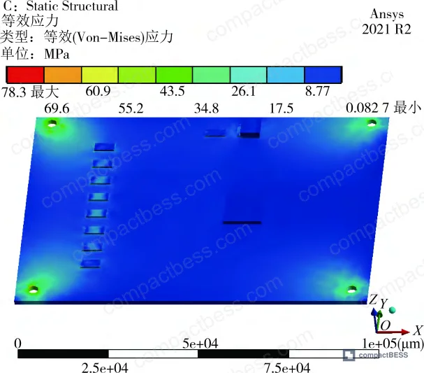
This is where single-module analysis falls short. Thermal stress in a constrained PCBA isn’t generated only by the hottest component — it’s generated by the interaction between temperature gradients, differential thermal expansion coefficients across dissimilar materials, and mechanical boundary conditions. A BMS board bolted into its enclosure through four M3 corner fasteners is a mechanically constrained system, and that constraint pattern directly shapes where stress concentrates.
Thermal stress results from the simulation:
- Maximum thermal stress on the entire board: 78.3 MPa — occurring at the M3 bolt hole corners, where the fixed boundary constraint completely prevents local thermal expansion
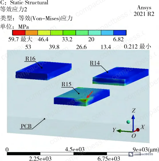
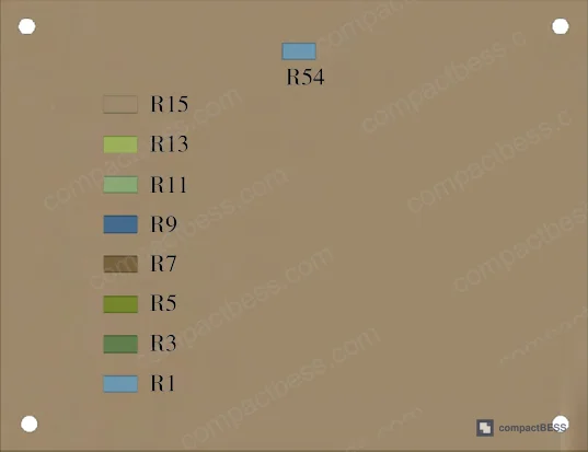
- Non-working balancing resistor R15 (rear face): 59.7 MPa at its PCB contact corner — stress concentration from differential expansion between alumina ceramic resistor body and FR-4 substrate
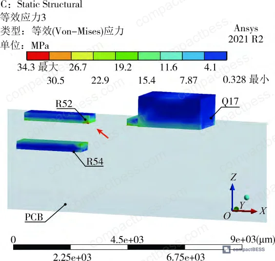
- Power supply resistor R52 (adjacent to Q17): 34.3 MPa at PCB contact corner
Honestly, the R15 finding is the most operationally important number in this analysis. R15 isn’t even actively dissipating power during balancing — it’s a passive component on the reverse side of the board, experiencing stress purely because of thermal gradients imposed by its active neighbors. If you’re spec-checking a BMS for field reliability, the resistors you should be most concerned about aren’t the ones running hot. It’s the constrained components sitting at module edges, absorbing stress from nearby thermal sources.
Z-axis deformation is the metric that connects directly to solder joint fatigue life. The simulation results show:
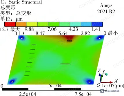
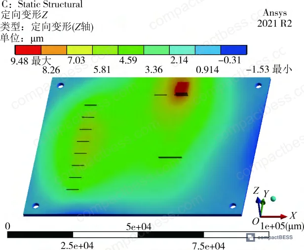
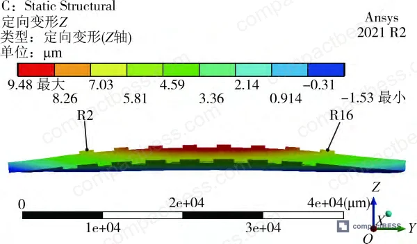
- Maximum Z-axis deformation: 9.5 μm at transistor Q17 location (power supply module)
- Deformation at M3 bolt hole locations: essentially zero (fixed constraint)
- Z-axis deformation increases monotonically with distance from the bolt holes
The pattern is counterintuitive at first — the maximum deformation isn’t at the hottest spot (balancing module at 54.4 °C) but at the power supply transistor Q17. This is because Q17 is positioned closer to the board center, further from the fixing constraints, allowing freer thermal expansion. The balancing module, while hotter, sits closer to board edges where the bolt constraints suppress deformation but amplify stress.
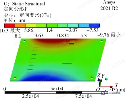
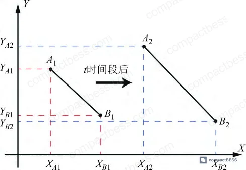
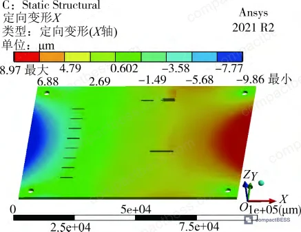
Experimental displacement measurement using digital optical microscopy confirmed X-axis deformation of 3–4 μm and Y-axis deformation of 7–11 μm in the Q17 region, with simulation-to-experiment mean error below 25%. The Y-axis deformation being 2–3× larger than X-axis deformation reflects the board’s aspect ratio and the relative proximity of constraints in each axis direction.
Most procurement teams don’t realize that thermal-mechanical reliability standards for automotive electronics — including IEC 62619 for industrial battery systems and the requirements embedded in ISO 26262 functional safety — do not specify board-level warpage limits or solder joint stress thresholds directly. Those limits exist in component-level standards like IPC-9701A for solder joint reliability testing, and very few BMS suppliers have this data. That gap between system-level safety certification and component-level mechanical reliability testing is where long-term field failures originate.
Thermal-Mechanical Failure Modes in BMS PCBA: What Qualification Testing Misses #
In supplier qualification work, the failure pattern follows a predictable sequence that infrared spot-checks during incoming inspection will not catch. The board looks fine thermally — temperatures are within the component’s rated range, and the MCU is running cool. The damage is accumulating at solder joints under edge resistors and at constrained mounting corners, driven by cyclic thermal stress from charge-discharge cycles, and it becomes visible only after hundreds or thousands of cycles.
Three specific failure initiation sites, in order of severity based on the stress data:
1. M3 bolt hole corners (78.3 MPa peak stress): The mechanical constraint interacts with thermal expansion to create the highest stress on the board. This is a board-level assembly design issue — if a supplier is mounting the BMS PCBA rigidly in all four corners without any compliance in the mounting scheme, they’re pre-loading the board’s worst stress concentration sites.
2. Balancing module edge resistors — rear face (59.7 MPa): The non-active resistors on the back of the balancing module experience stress concentration at their PCB interface corners. In a 16S balancing configuration with alternating resistor switching, these components cycle between loaded and unloaded states, driving fatigue accumulation.
3. Power supply module resistors adjacent to Q17 (34.3 MPa): Secondary stress concentration from proximity to the highest single-component power dissipator on the board.
In supplier qualification, we’ve seen boards that pass standard BMS electrical performance tests — voltage measurement accuracy, balancing current, communication integrity — but show solder joint micro-cracking under cross-section analysis after accelerated thermal cycling per IEC 60068-2-14 (thermal shock, -40 °C to +85 °C). The correlation between initial thermal stress concentration and early solder joint failure is direct.
Practical Guidance for Buyers #
When you’re evaluating a BMS supplier’s thermal design documentation, the key question is whether their analysis covers multi-module interactions or only the MCU. Single-chip thermal analysis is easy to produce and tells you almost nothing about board-level reliability. The relevant data is the temperature differential across the full PCBA under worst-case balancing load — if that number exceeds 20 °C on a naturally cooled board, the supplier needs to demonstrate that their PCB layout, component placement, and mounting scheme have been designed to manage resulting thermal stress, not just temperature.
For 16S or higher series-count BMS designs, the balancing module is the primary heat source and the design decision that has the most leverage on reliability is balancing resistor placement — specifically, whether the layout creates a thermal accumulation zone at the array center. Parabolic temperature profiles across the resistor array (hotter in the center) indicate suboptimal spacing and are predictive of early edge-component stress failures.
For any BMS board with a linear LDO-based power supply stepping down from high pack voltage to MCU supply voltage, the transistor dissipation problem is structural — the power loss is determined by the voltage differential, not the design skill of the layout engineer. Suppliers using switching regulators instead of LDO circuits for the pack-to-MCU supply will show significantly lower thermal stress in the power module.
At compactbess.com, we work directly with qualified Chinese BMS manufacturers supplying global OEM buyers across automotive, industrial, and portable power applications — our sourcing team can connect you with manufacturers that maintain multi-module thermal simulation reports and IPC-9701A solder reliability data as standard qualification documentation.
Need help identifying qualified suppliers for BMS modules with validated thermal-mechanical reliability data? Talk to our sourcing team →
Supplier Qualification Questions #
- Can you provide a full-board thermal simulation report showing peak temperature at the balancing module resistor array center, with maximum board temperature differential documented — and does that differential stay below 20 °C under maximum balancing load at 25 °C ambient?
- What is the maximum Z-axis thermal deformation at the highest-dissipation component on your BMS board, measured or simulated under natural convection boundary conditions — and is that value below 10 μm under your rated operating load?
- For your balancing module, what is the peak thermal stress at the SMD resistor-to-PCB contact corners on the board’s rear face (non-active resistors), and have you cross-referenced this against IPC-9701A solder joint fatigue thresholds?
- Does your LDO or power supply module use a linear (NPN transistor) architecture or a switching regulator — and if linear, what is the steady-state transistor temperature under full pack voltage input with 5 V MCU supply output at maximum rated pack voltage?
- Has your BMS PCBA been subjected to accelerated thermal cycling per IEC 60068-2-14 (thermal shock, -40 °C to +85 °C, minimum 200 cycles), and can you provide cross-section photomicrographs of balancing module edge resistor solder joints post-cycling?
Sourcing Checklist #
- [ ] Supplier provides multi-module thermal simulation report covering balancing, power supply, control, and communication modules simultaneously — not single-module analysis only
- [ ] Board-level peak temperature differential documented as ≤20 °C under maximum balancing load at 25 °C ambient natural convection
- [ ] Peak Z-axis thermal deformation at power supply transistor confirmed ≤10 μm under rated operating conditions
- [ ] Thermal stress at edge balancing resistor solder joint corners documented — reference IPC-9701A for acceptable fatigue margin
- [ ] Simulation model validated against physical measurement (infrared thermography or equivalent) with temperature prediction error ≤7% across all major heat sources
- [ ] PCB mounting scheme reviewed — flexible or compliant mounting hardware specified if four-corner rigid bolting is used, to reduce constraint-driven stress at bolt hole locations
- [ ] Supplier can confirm balancing module resistor layout avoids thermal accumulation at array center (temperature profile across resistor array provided)
- [ ] Product-level IEC 62619 compliance documentation available, supplemented by component-level solder reliability data per IPC-9701A
Key Specifications Table #
| Parameter | Recommended Value | Verification Method |
|---|---|---|
| Board-level temperature differential under max balancing load | ≤20 °C | Infrared thermography (emissivity 0.95) at steady-state, 25 °C ambient, natural convection |
| Peak balancing module temperature (SMD resistor center) | ≤55 °C at rated load, 25 °C ambient | Simulation (ANSYS Icepak or equivalent) validated against thermal imaging; error ≤7% |
| Maximum Z-axis thermal deformation at power supply module | ≤10 μm | FEA structural analysis (ANSYS Mechanical or equivalent); cross-check with digital optical microscopy |
| Peak thermal stress at edge balancing resistor solder joints | Reference against IPC-9701A fatigue data; flag if >60 MPa | Coupled thermal-structural FEA simulation; report stress at PCB-resistor contact corners |
| Simulation-to-measurement temperature error | <7% across all major heat sources | Validate against infrared thermography at ≥5 component locations |
| Balancing resistor power dissipation (active resistors) | Document per design; typical ≤250 mW per component for 16S SMD resistor balancing | Component datasheet cross-reference + thermal simulation |
Can’t find a supplier meeting these specs? Submit your requirements and we’ll match you within 48 hours.
Frequently Asked Questions #
Q: Why does the balancing module reach higher temperatures than the power supply transistor, even though Q17 has higher single-component power dissipation at 407.4 mW versus 235.2 mW per balancing resistor?
A: Because thermal accumulation is a density effect, not a single-component effect. The balancing module operates multiple resistors simultaneously within a compact spatial array. Heat from neighboring resistors converges at the array center, and the small surface area of SMD chip resistors limits convective dissipation. Q17, despite dissipating more power as a single component, operates in relative thermal isolation and can shed heat more effectively. This is why multi-module simulation is necessary — single-resistor or single-transistor analysis will always underestimate the hottest point on the board.
Q: Is a 9.5 μm Z-axis deformation actually significant enough to cause solder joint failure?
A: On its own, a single thermal event producing 9.5 μm deformation is unlikely to cause immediate failure. The problem is cyclic fatigue. A BMS board in an EV application experiences hundreds to thousands of charge-discharge cycles per year, each driving a thermal excursion. Solder joint fatigue failure is driven by the accumulated plastic strain range per cycle, and even sub-10 μm deformations at constrained solder joints can initiate micro-cracks within a few hundred cycles under aggressive cycling profiles. The combination of 59.7 MPa stress at edge resistor joints with cyclic deformation is the failure mechanism to design against.
Q: Can forced air cooling eliminate the thermal stress problem?
A: It reduces peak temperature, which reduces the absolute magnitude of thermal deformation — but it doesn’t eliminate the differential expansion problem. The balancing resistors, PCB substrate (FR-4), and MCU encapsulation resin all have different coefficients of thermal expansion. The FR-4 PCB has CTE values of 15.0 ppm/°C in-plane (XY) and 55.0 ppm/°C through-thickness (Z), while alumina ceramic resistors sit at approximately 6.9 ppm/°C. That mismatch exists at any operating temperature, and forced cooling that creates steep temperature gradients can actually worsen local stress distribution even while lowering average temperature.
Q: Our BMS supplier says they only test the MCU temperature. Is that sufficient?
A: No. The MCU in this analysis runs at 38.2 °C — the coolest major component on the board. Testing only MCU temperature gives you the best-case thermal reading on a board where the real reliability risks are at 54.4 °C (balancing module) and 59.7 MPa solder joint stress (edge resistors). It’s a useful indicator for software performance, not for board-level mechanical reliability.
Q: Which BMS functional modules need priority attention for thermal management design?
A: In descending order of thermal-mechanical risk: (1) balancing module — highest temperature and most complex multi-component interaction; (2) power supply module — highest single-component deformation and significant adjacent component stress; (3) MCU/control module — lower temperature but sensitive to board warpage if mounted near the balancing module boundary. Communication modules in this configuration showed negligible thermal loading.
Published by compactbess.com Technical Team | Request a sourcing quote
For deeper context on BMS protection circuit design considerations, see our protection circuit design reference and BMS communication protocols guide.
Data source: Multi-Module Thermal-Stress Coupled Modeling and Reliability Analysis of Battery Management System Circuit Boards, L. Chen et al., Journal of the Electrochemical Society, 2024
Content reviewed by elena.fischer | © compactbess.com — All rights reserved. Unauthorized reproduction prohibited.


