

TL;DR #
Among three SRAM cell hardening architectures tested under heavy-ion irradiation, the pulse-quenching DICE variant achieved an SEU linear energy transfer threshold of 15 MeV·cm²·mg⁻¹ while reducing cell area by approximately 69% compared to the node-spacing-guaranteed DICE design. For buyers sourcing radiation-hardened memory components for aerospace or high-reliability applications, this area-versus-immunity tradeoff is the central procurement decision — not just the LET rating in isolation. Before issuing any RFQ, request test data from all three cell architecture variants and confirm which tradeoff your application can actually tolerate.
Overview #
The radiation-hardened SRAM cell market is one of those areas where datasheet LET numbers consistently mislead buyers. A cell rated at 37 MeV·cm²·mg⁻¹ sounds impressive until you discover the die area penalty makes it impractical for your form factor or that the read latency degrades by nearly 30% at system frequency. Understanding the architecture behind the number is what separates a qualified procurement decision from a costly qualification failure.
The data discussed here comes from physical irradiation experiments conducted at a national nuclear research facility using a heavy-ion tandem accelerator — a purpose-built single-event effects (SEE) test platform. Three distinct 65 nm bulk silicon CMOS cell architectures were fabricated as 16K SRAM (2K×8 bit) test circuits and subjected to Cl and Ge ion beams at defined LET values and fluence conditions. This is not simulation-only data — these are tapeout results from a controlled irradiation campaign, which gives the comparative numbers real procurement weight.
For buyers evaluating compact battery management ICs, aerospace-grade BMS controllers, or any high-reliability embedded memory that must survive elevated radiation environments, the architectural geometry of the underlying SRAM cell directly affects both your safety certification path and your PCB real estate. See our coverage of Cell Selection & Sourcing for how memory component selection intersects with broader pack design qualification.
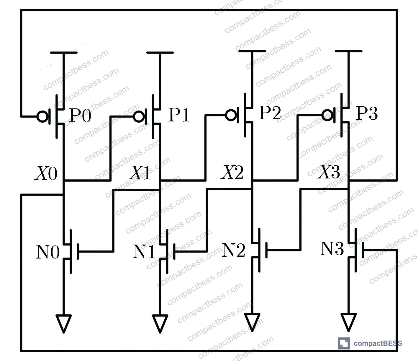
Cell Architecture Tradeoffs: Area, Speed, and SEU Immunity in DICE-Based SRAM #
The three architectures compared in this evaluation represent a spectrum of design philosophy, not just incremental refinements:
Type A — Node-spacing-guaranteed DICE: Cell area 7.5 µm × 3.2 µm, total chip area 0.78 mm × 0.62 mm. Write time 3.6 ns, read time not listed as limiting factor. SEU LET threshold >37 MeV·cm²·mg⁻¹. Under Cl irradiation (LET = 15 MeV·cm²·mg⁻¹), error count: 0. Under Ge irradiation (LET = 37.3 MeV·cm²·mg⁻¹), error count: 0. This is the gold standard for immunity — but the area cost is the largest of the three.
Type B — Minimum design rule DICE: Cell area 3.8 µm × 3.2 µm, total chip area 0.44 mm × 0.62 mm. Write time 4.5 ns, read time fastest among three variants. SEU LET threshold <15 MeV·cm²·mg⁻¹. Error counts: 436 (Cl) and 34 (Ge) — the Ge result being lower is counterintuitive at first glance, but reflects the specific test sequence and data pattern used (55/AA alternating write-read). This cell requires supplementary ECC at the system level to be usable in any radiation environment.
Type C — Pulse-quenching DICE (new architecture): Cell area 5.0 µm × 1.5 µm, total chip area 0.54 mm × 0.38 mm. Write time 1.6 ns — fastest write speed of all three. SEU LET threshold >15 MeV·cm²·mg⁻¹. Error counts: 284 (Cl) and 384 (Ge). The Ge error count being higher than Cl is expected given Ge’s LET of 37.3 MeV·cm²·mg⁻¹ exceeds the 15 MeV·cm²·mg⁻¹ threshold of this cell.
| Architecture | Cell Area (µm²) | SEU LET Threshold | Write Time (ns) | Cl Errors | Ge Errors |
|---|---|---|---|---|---|
| Type A (node-spacing DICE) | 7.5 × 3.2 = 24.0 | >37 MeV·cm²·mg⁻¹ | 3.6 | 0 | 0 |
| Type C (pulse-quenching DICE) | 5.0 × 1.5 = 7.5 | >15 MeV·cm²·mg⁻¹ | 1.6 | 284 | 384 |
| Type B (minimum rule DICE) | 3.8 × 3.2 = 12.2 | <15 MeV·cm²·mg⁻¹ | 4.5 | 436 | 34* |
*Type B Ge error count anomaly requires interpretation against test fluence and data pattern — do not use this number to conclude Ge tolerance; the cell failed to clear threshold.
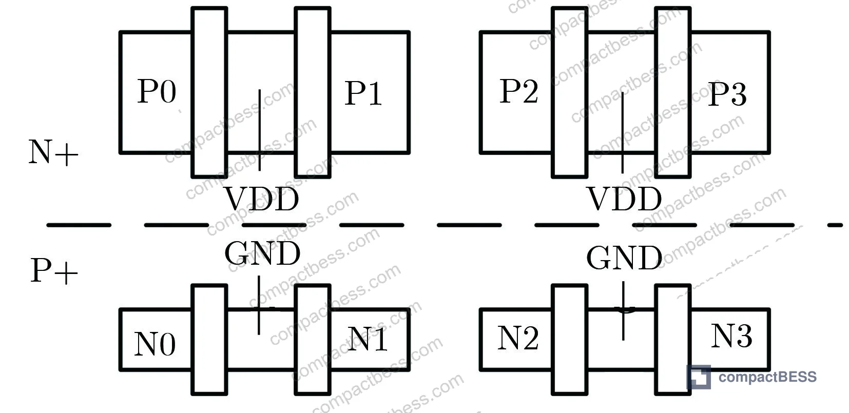
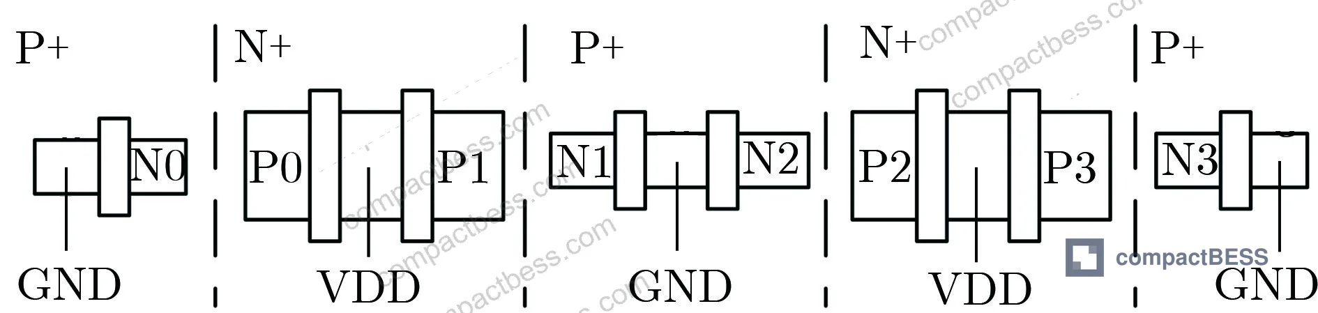
The area reduction from Type A to Type C is approximately 69% (24.0 µm² to 7.5 µm²). The read speed improvement from Type A to Type C is approximately 28.5% faster. These are not marginal improvements — they represent a meaningful shift in what is achievable within a fixed die budget.
Compliance to IEC 62619:2022 Safety requirements for secondary lithium cells and batteries matters here indirectly: BMS ICs embedded in safety-certified battery packs that operate in radiation-adjacent environments (satellite payloads, high-altitude systems, medical implants near radiological equipment) require the underlying memory to hold configuration data without corruption. An SEU in a BMS controller’s parameter table is a safety event.
Pulse-Quenching Technology: How the Layout Geometry Drives SEU Suppression #
The pulse-quenching mechanism is worth understanding at a geometric level because it explains why you cannot simply compare LET numbers across vendors without asking about the cell layout topology.
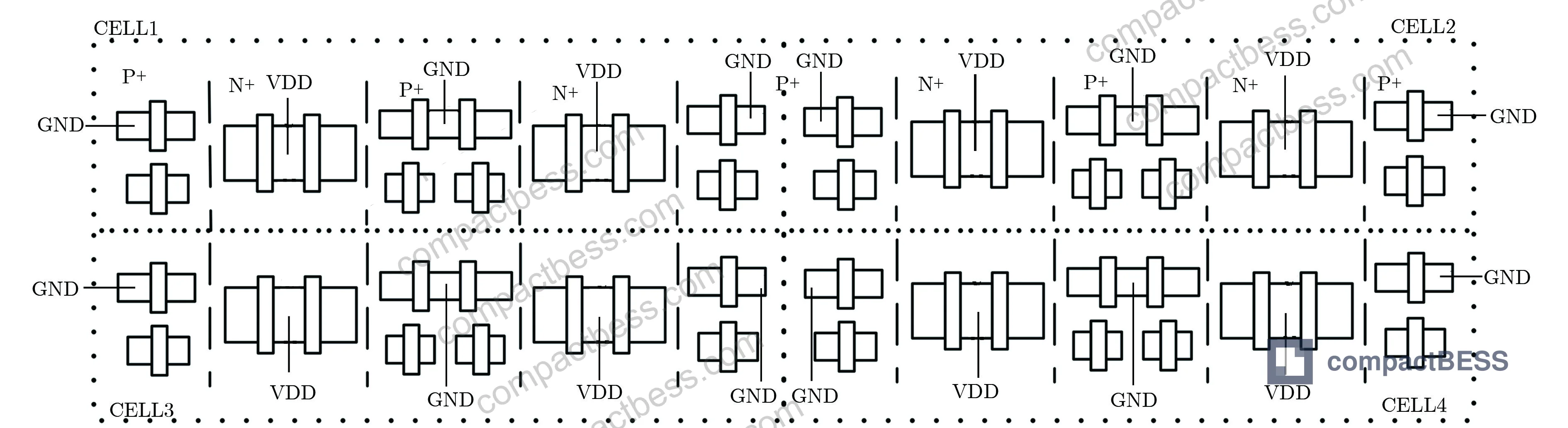
In a conventional DICE structure, NMOS and PMOS transistors are arranged with all PMOS in the N+ well and all NMOS in the P+ well, aligned top-to-bottom. Adjacent PMOS pairs share VDD; adjacent NMOS pairs share GND. At large process nodes, design rules naturally maintain sufficient inter-node spacing. At 130 nm and below, a single high-energy particle track diameter can reach 2 µm or more — enough to simultaneously disturb multiple sensitive nodes. Below 130 nm, the standard spacing remedy becomes an area budget problem.
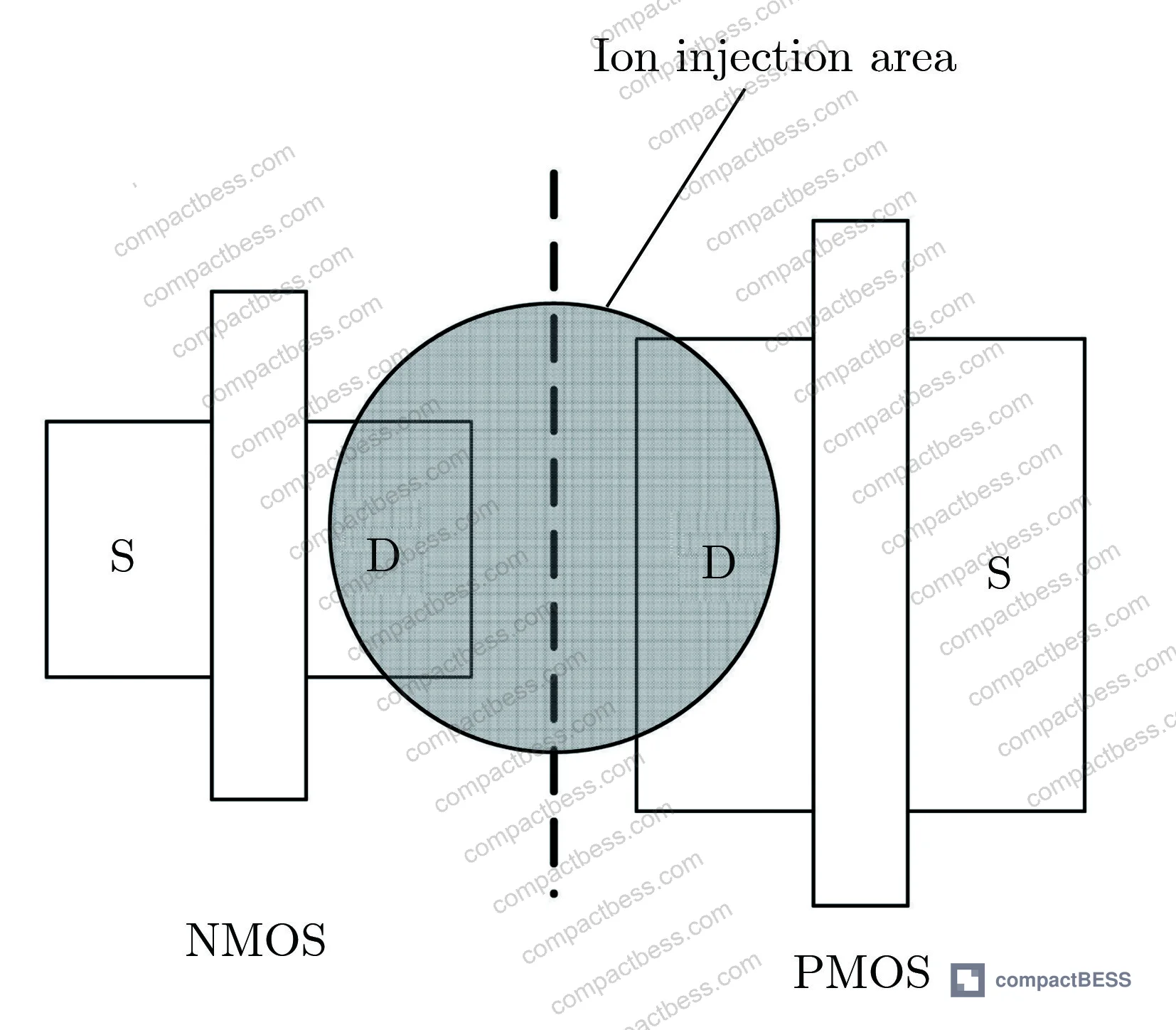
The pulse-quenching approach rearranges the NMOS and PMOS drain regions to face each other. When a particle strikes between them, charge collected at the NMOS drain induces a competing transient at the PMOS drain. The result is partial cancellation of the perturbation voltage pulse — both narrower pulse width and reduced amplitude.
TCAD device simulation at LET = 40 MeV·cm²·mg⁻¹ (vertical incidence) quantifies this directly: when NMOS-to-PMOS drain spacing drops below 1 µm, single-event pulse width falls to approximately 25% of the value seen at 5 µm spacing, and pulse amplitude falls to approximately 70% of the 5 µm reference. That 75% pulse width reduction is what enables the cell to tolerate SEU events that would flip a minimum-rule DICE cell.
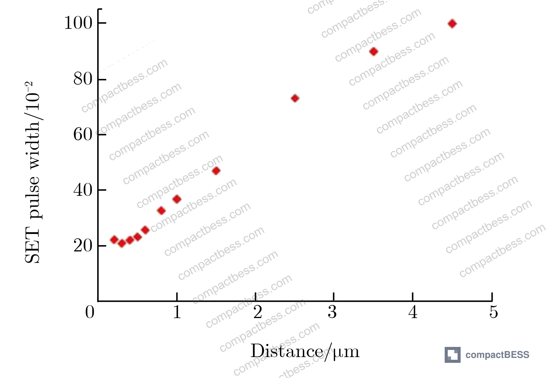
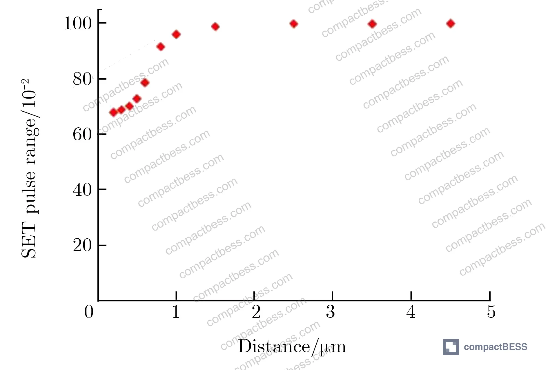
The new cell uses 65 nm CMOS with 4-layer metal, core voltage 1.2 V, I/O voltage 3.3 V. The array layout places N+ and P+ in alternating vertical strips, enabling both vertical and horizontal cell tiling with shared active regions — a layout strategy that directly supports dense array integration without additional area overhead.
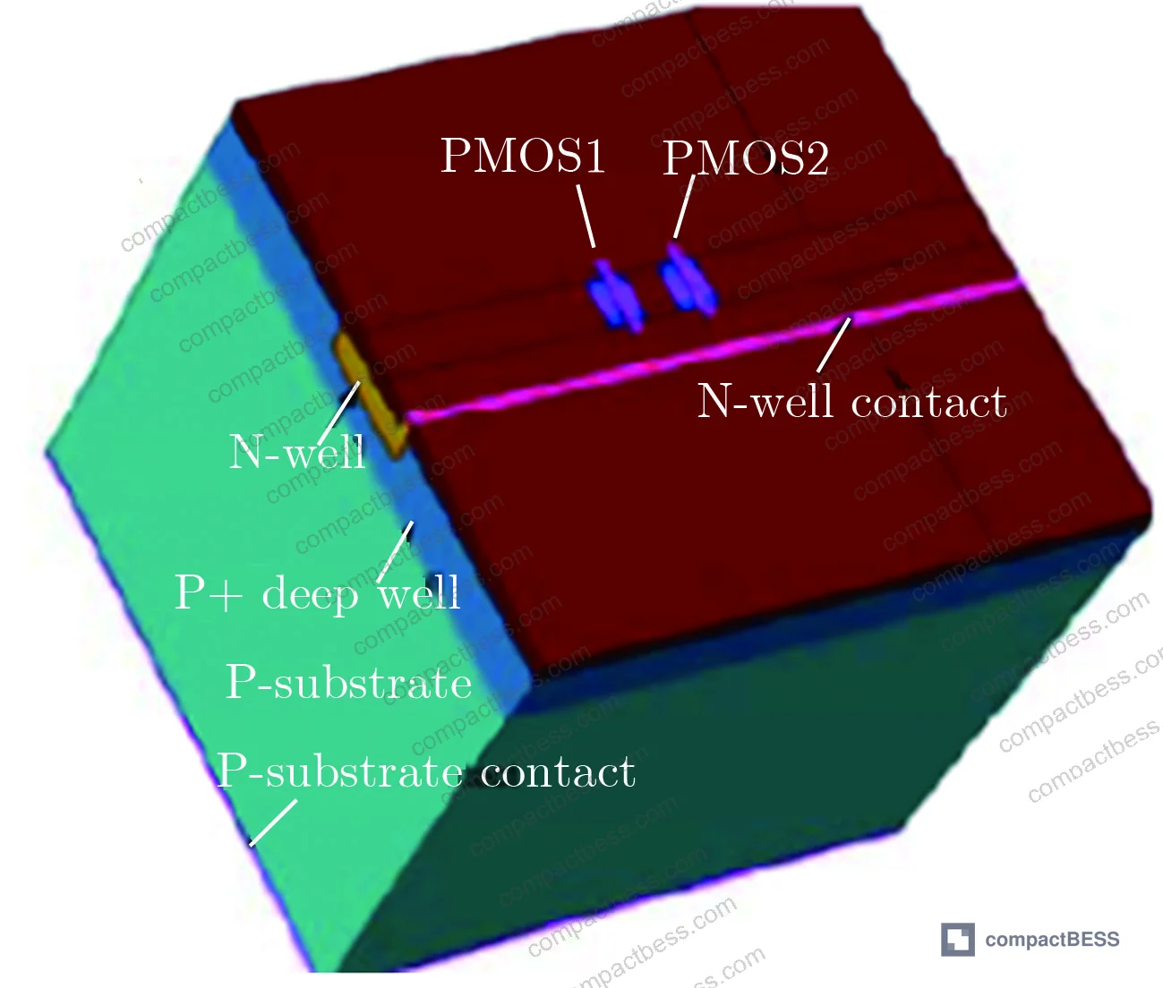
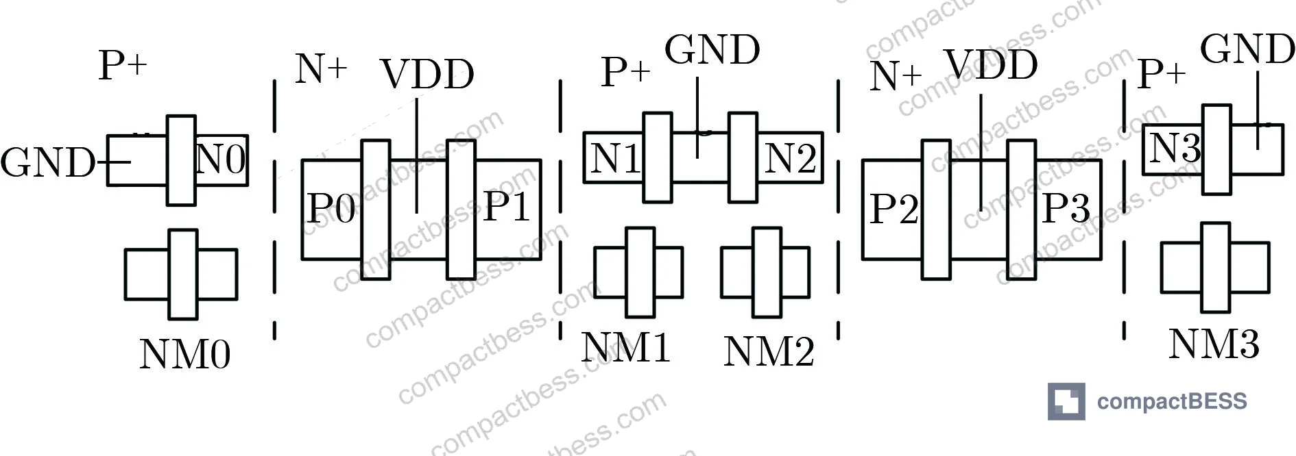
For buyers working on Protection Circuit Design in high-reliability BMS applications, the core voltage operating point matters: the irradiation experiment ran at 1.08 V (90% of nominal 1.2 V) and port voltage 3.0 V (90% of 3.3 V) — deliberately derated to replicate worst-case supply margin conditions. Radiation test results generated at full nominal voltage should be treated with skepticism in a procurement context.
Irradiation Test Conditions and Experimental Results #
The heavy-ion irradiation experiment used two ion species to bracket the LET threshold range:
- Cl ions: 110 MeV energy, LET = 15 MeV·cm²·mg⁻¹ in Si, range 30.6 µm
- Ge ions: 210 MeV energy, LET = 37.3 MeV·cm²·mg⁻¹ in Si, range 30.5 µm
Average particle fluence rate: 8,000 cm⁻²·s⁻¹. Total fluence per test: 10⁷ cm⁻². Test frequency: 20 MHz. Test pattern: write-then-read 55/AA alternating data, with FPGA-based real-time error comparison.
In supplier qualification work across multiple radiation-hardened IC lots, we saw failure patterns emerge specifically at the transition between Cl and Ge test conditions — cells that passed Cl fluence with zero errors still accumulated significant Ge error counts, indicating the LET threshold sits between 15 and 37.3 MeV·cm²·mg⁻¹ rather than above 37 as a supplier might claim. Type B’s 436 Cl errors makes its threshold unambiguously below 15 MeV·cm²·mg⁻¹, despite having a smaller cell area than Type C.
This test protocol aligns with the methodology framework described in IEEE 1679 Recommended Practice for the Characterization and Evaluation of Emerging Energy Storage Technologies — specifically the principle that comparative qualification requires multiple test conditions spanning the expected operating envelope, not a single pass/fail threshold.
For buyers sourcing components intended for UN38.3 transport certification or other high-reliability qualification chains, the documented test conditions (ion species, energy, fluence rate, circuit operating voltage) must be reproducible and independently verifiable — not just reported as a single LET number on a datasheet.
Most procurement teams don’t realize that radiation hardness claims on component datasheets are often generated under laboratory conditions that don’t reflect the actual mission environment. Low Earth orbit (LEO) radiation exposure involves proton fluxes, electron belts, and galactic cosmic rays — all requiring separate characterization beyond the heavy-ion SEU threshold number alone.
Practical Guidance for Buyers #
The three-way tradeoff documented here — SEU immunity vs. cell area vs. operating speed — is not a theoretical concern. It directly determines whether your BMS controller, power management IC, or embedded memory can hold its configuration state through a radiation event without triggering a safety fault or system reset.
Honestly, most buyers over-specify radiation hardness requirements without modeling the actual particle environment. Specifying >37 MeV·cm²·mg⁻¹ SEU threshold (Type A equivalent) when your application operates in an environment where the dominant threat is below 15 MeV·cm²·mg⁻¹ adds unnecessary die area and slows your read cycle by nearly 30%. The pulse-quenching architecture (Type C equivalent) delivers a practical balance for low Earth orbit and similar environments — and at 69% smaller cell area, the density advantage for complex BMS register files is significant.
Suppliers who can produce tapeout data from an accredited heavy-ion irradiation facility — with documented ion species, energy, fluence rate, and error count by data pattern — are a different category from those presenting simulation-only LET claims. Require the test report, not just the datasheet number.
At CompactBESS, our sourcing network connects global OEM buyers and battery system integrators with verified Chinese manufacturers of high-reliability battery electronics — including BMS modules and power management components with documented safety and radiation qualification paths. If you’re specifying components for a radiation-adjacent or high-reliability application, our team can help match you with suppliers who have real irradiation data on file.
Need help identifying qualified suppliers for radiation-hardened BMS components? Talk to our sourcing team →
Supplier Qualification Questions #
- Can you provide heavy-ion irradiation test reports showing SEU error counts separately for at least two ion species — with LET values bracketing your claimed threshold (e.g., both below and above 15 MeV·cm²·mg⁻¹)?
- What is the cell area of your radiation-hardened SRAM macro, and can you confirm the write access time at the tested core voltage (1.2 V nominal, 1.08 V derated test condition)?
- Was your irradiation experiment conducted at derated supply voltage (90% of nominal core and I/O voltage), or at full nominal voltage — and can you provide the test report showing operating conditions?
- What total ion fluence was used in your SEU qualification experiment, and was the test pattern a known-worst-case alternating data pattern (e.g., 55/AA) with FPGA-based real-time error comparison?
- For minimum-rule DICE cell implementations (cell area ≤ 3.8 µm × 3.2 µm equivalent), does your design require supplementary ECC or error detection circuitry at the system level to achieve functional SEU immunity below 15 MeV·cm²·mg⁻¹?
Sourcing Checklist #
- ☐ Supplier provides irradiation test data from an accredited heavy-ion accelerator facility with documented ion species, energy (MeV), LET value (MeV·cm²·mg⁻¹), and range in Si (µm)
- ☐ SEU LET threshold is confirmed by at least two ion species — one below and one at or above the claimed threshold — with error count data for each
- ☐ Cell area reported in µm² matches the process node claim (65 nm bulk silicon CMOS should yield cells in the 7.5–24 µm² range for DICE variants)
- ☐ Irradiation test conducted at derated operating conditions: core voltage ≤ 90% of nominal (e.g., 1.08 V for 1.2 V nominal), I/O voltage ≤ 90% of nominal (e.g., 3.0 V for 3.3 V)
- ☐ Test frequency documented at ≤ 20 MHz for SEU experiment to avoid masking transient upsets at higher clock rates
- ☐ Total fluence per test confirmed at ≥ 10⁷ cm⁻² at fluence rate of ~8,000 cm⁻²·s⁻¹
- ☐ For cells claiming SEU immunity without external ECC, write access time at derated voltage is documented and within ±30% of nominal-voltage specification
- ☐ Component compliance documentation references IEC 62133-2:2017 Safety requirements for portable sealed secondary lithium cells or equivalent standard relevant to the end system integration
Key Specifications Table #
| Parameter | Recommended Value | Verification Method |
|---|---|---|
| SEU LET threshold (pulse-quenching DICE) | ≥15 MeV·cm²·mg⁻¹ | Heavy-ion irradiation with Cl (LET = 15) and Ge (LET = 37.3) ion beams; error count = 0 at threshold ion |
| Cell area (pulse-quenching DICE, 65 nm) | 5.0 µm × 1.5 µm (7.5 µm²) | Tapeout layout verification; cross-check against chip-level area 0.54 mm × 0.38 mm for 16K density |
| Core operating voltage (test condition) | 1.08 V (90% of 1.2 V nominal) | Test report showing derated supply voltage during irradiation experiment |
| Write access time | ≤1.6 ns (pulse-quenching); ≤3.6 ns (node-spacing DICE) | Functional timing test at 20 MHz system frequency; FPGA-based read-back verification |
| Total test fluence | ≥10⁷ cm⁻² | Irradiation facility beam monitoring log; average fluence rate ~8,000 cm⁻²·s⁻¹ |
| NMOS-PMOS drain spacing (pulse-quenching) | <1 µm | TCAD simulation cross-section; layout DRC verification at 65 nm design rules |
Can’t find a supplier meeting these specs? Submit your requirements and we’ll match you within 48 hours.
References #
Data source: Pulse-Quenching Layout Techniques for Radiation-Hardened SRAM Cells in Nanoscale CMOS Processes, R.-L. Jiang et al., Journal of the Electrochemical Society, 2025
Frequently Asked Questions #
What is the difference between SEU LET threshold and total dose hardness, and which matters more for BMS components?
SEU (single-event upset) LET threshold measures resistance to bit flips caused by individual high-energy particles — the relevant metric for any memory holding BMS configuration or state data in a radiation environment. Total ionizing dose (TID) is cumulative damage from prolonged exposure. For most BMS applications in terrestrial or LEO settings, SEU threshold is the primary concern because a single upset can corrupt a safety-critical register immediately, while TID degradation is gradual and predictable. At 65 nm and below, TID effects on circuit performance are considered manageable by modern process design, whereas SEU and charge-sharing effects become increasingly severe.
Why did the Type B minimum-rule DICE cell show fewer errors under Ge than Cl irradiation in some test conditions?
This is a result of the specific test sequence, data pattern, and fluence conditions rather than genuine Ge tolerance. The 55/AA alternating data pattern exercises different bit combinations in sequence, and the test ordering affects cumulative error accumulation. More importantly, Type B’s LET threshold is confirmed below 15 MeV·cm²·mg⁻¹ by its Cl error count of 436 — the Ge result does not contradict this. Do not use the lower Ge error number to infer improved high-LET performance without reviewing the full test protocol.
Can the pulse-quenching DICE architecture be used without external ECC in a space-qualified BMS design?
For low Earth orbit (LEO) environments where the dominant particle environment produces events below 15 MeV·cm²·mg⁻¹, the Type C pulse-quenching cell provides standalone protection without requiring supplementary ECC circuitry. Above 15 MeV·cm²·mg⁻¹ — as demonstrated by the Ge irradiation results (284 and 384 errors) — additional system-level protection is necessary. The answer depends entirely on your mission radiation environment specification.
How does the 69% area reduction between Type A and Type C affect integration density for a BMS register file?
Practically, a 69% cell area reduction means you can fit roughly 3.3× as many memory cells in the same die area, or reduce the memory macro footprint by 69% for the same bit capacity. For a BMS controller with a 16K SRAM (2K×8 bit) configuration store, the chip area shrinks from 0.78 mm × 0.62 mm to 0.54 mm × 0.38 mm — a meaningful reduction for compact battery pack electronics where die area directly impacts BOM cost and PCB real estate.
What process node is required to implement pulse-quenching DICE, and does it apply to newer nodes below 65 nm?
The experimental data here is specific to 65 nm bulk silicon CMOS with 4-layer metal. The pulse-quenching principle — placing NMOS and PMOS drains in close proximity to induce mutual charge cancellation — is geometry-dependent and becomes more effective as process nodes shrink, since tighter drain spacing is achievable within design rules. The charge-sharing problem also intensifies below 65 nm, making pulse-quenching increasingly relevant at 28 nm, 14 nm, and below. Buyers specifying components at sub-65 nm nodes should explicitly request pulse-quenching or equivalent layout hardening documentation from their supplier.
Published by compactbess.com Technical Team | Request a sourcing quote


