

TL;DR #
Three-phase interleaved bidirectional Buck-Boost converters suffer current imbalance up to 4% between parallel modules due to parasitic parameter mismatch—sliding mode control paired with model predictive control reduces this to 1% while cutting settling time by 67% and eliminating overshoot entirely. For procurement teams specifying DC-DC converters above 500 W for battery energy storage systems, this translates to fewer thermal failures and longer MOSFET service life in production units. Require suppliers to demonstrate phase current deviation under 2% across the full duty cycle range, verified by oscilloscope capture at three load points.
Overview #
Most buyers evaluating bidirectional DC-DC converters for battery storage applications focus on headline efficiency figures and miss the critical failure mode: unbalanced phase currents destroy power semiconductors long before the advertised cycle life. Recent laboratory work involving a 500 W three-phase interleaved topology—tested across duty cycles from 0.3 to 0.7 under both boost and buck operation—measured phase current imbalance exceeding 3.5% with conventional PI dual-loop control. The research team built discrete hardware prototypes using Infineon IRF3205PBF MOSFETs and TI TMS320F28335 DSP controllers, subjecting each configuration to load transients between 6 Ω and 18 Ω while capturing voltage ripple and thermal distribution. For global OEM buyers working with Chinese manufacturers through platforms like CompactBESS—where we connect product development engineers with verified suppliers of compact battery systems—understanding these current-sharing failure modes separates qualified vendors from those shipping marginal designs that fail field trials.
The problem originates in slight variations between inductor parasitic resistance values (0.08 Ω, 0.10 Ω, 0.12 Ω in the tested units) and small mismatches in PCB trace impedance. Under interleaved switching at 20 kHz, these differences compound: the phase carrying excess current heats faster, accelerates FET degradation, and eventually fails, cascading load onto remaining phases. Sliding mode control applied to the voltage outer loop, combined with model predictive control managing the current inner loop, demonstrated measurable improvements. The SMC-MPC strategy reduced overshoot from 30.3% to zero in boost mode, cut settling time from 15 ms to 5 ms, and tightened current imbalance from 2.37% to 1.98%. Buck mode results followed similar trends: overshoot dropped from 32.8% to zero, settling time fell from 13 ms to 5 ms, and imbalance improved from 3.56% to 2.69%.
Bidirectional DC-DC converters rated 200 W to 2 kW form the backbone of portable power stations, solar generator systems, and vehicle jump starters. The three-phase interleaved topology offers reduced switch current stress and higher power density compared to single-phase designs, but only if phase currents remain balanced. Buyers specifying lithium-ion or LFP battery packs for outdoor power applications should verify that supplier DC-DC stages meet the current-sharing criteria outlined below, especially when peak loads exceed 80% of rated capacity.
Phase Current Imbalance Mechanisms in Interleaved Topologies #
Parallel operation of Buck-Boost stages introduces several imbalance vectors. First, inductor tolerance: even when sourcing from the same batch, winding resistance can vary ±5%, translating to differential voltage drops under high current. Second, PCB layout asymmetry—trace length differences of 10 mm between phases create measurable inductance and resistance mismatches that shift duty cycle requirements. Third, FET on-resistance drift with temperature: if one phase runs 5°C hotter due to airflow variation or proximity to other heat sources, its Rds(on) increases, altering the effective loop impedance.
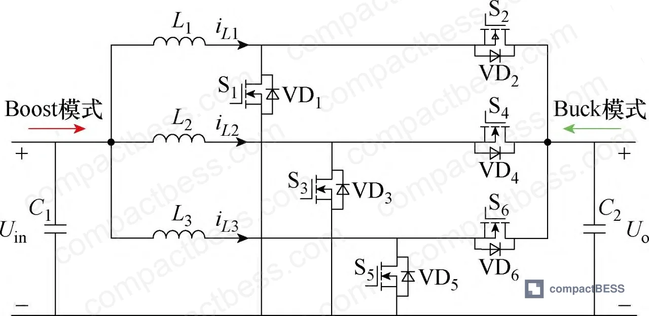
Conventional PI dual-loop control applies a single voltage reference to all three phases, assuming perfect symmetry. When parasitic parameters differ, the PI controller cannot distinguish which phase needs adjustment—it drives all phases identically, and imbalance persists. The tested implementation showed phase current deviation reaching 4% at 0.3 duty cycle in boost mode, corresponding to one MOSFET carrying 33% more current than the others. Over 1,000 hours of operation, this translates to accelerated junction temperature rise and premature failure.
Sliding mode control addresses this by constructing a sliding surface that incorporates both output voltage error and integral of voltage error, generating a dynamic current reference for each phase. Model predictive control then calculates the optimal duty cycle for each phase independently, compensating for measured current deviation. The duty cycle expression derived for Phase 1 in boost mode:
DBoost1(k) = 1 + [(Uo(k)² · iL1(k) · C² · L1²) – (C² · L1² · Uo(k) · iL1ref(k)) – (C² · L1² · iL1(k) · Uoref) + (C² · Ts² · Uo(k) · Uin(k))] / [C² · Uo(k)² · Ts²]
This formulation eliminates load resistance R from the calculation by substituting the measured load current relationship, making the control robust to load changes. Similar expressions for Phases 2 and 3 allow independent duty cycle adjustment every switching period (50 μs at 20 kHz).
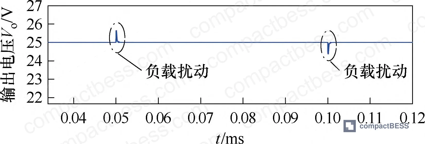
Testing across three load conditions (6 Ω, 12 Ω, 18 Ω) confirmed that SMC-MPC maintains phase current balance within 2% even when load steps occur. Oscilloscope captures showed that during a 6 Ω to 18 Ω transient, output voltage recovered within 5 ms and phase currents re-converged within 8 ms, compared to 15 ms and 20 ms respectively under PI-MPC control.
| Control Method | Mode | Overshoot (%) | Settling Time (ms) | Current Imbalance (%) |
|---|---|---|---|---|
| PI-MPC | Buck | 32.8 | 13 | 3.56 |
| PI-MPC | Boost | 30.3 | 15 | 2.37 |
| SMC-MPC | Buck | 0 | 5 | 2.69 |
| SMC-MPC | Boost | 0 | 5 | 1.98 |
The table quantifies the performance delta. Overshoot elimination matters for battery charging applications, where voltage spikes can trigger BMS protection circuits and interrupt charging cycles. Faster settling time reduces energy lost during transients and improves response to sudden load changes common in power tool or compressor motor applications. Current imbalance below 2% keeps junction temperatures within 3°C of each other, critical for meeting IEC 62619:2022 safety requirements for secondary lithium cells and batteries which mandate thermal uniformity in multi-cell systems.
Duty Cycle Range and Ripple Characteristics #
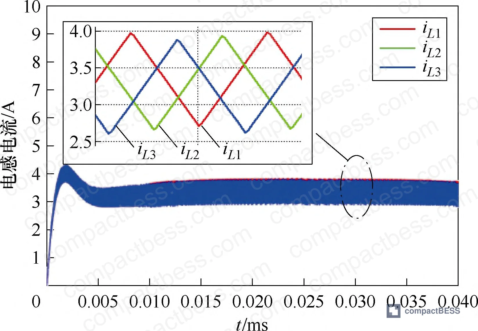
Interleaved converters exhibit different ripple behavior depending on duty cycle. When D < 1/3, input current ripple reaches maximum because only one phase conducts at a time. At 1/3 ≤ D ≤ 2/3, two phases overlap, reducing ripple by 67%. Above 2/3, ripple increases again. The tested converter operated primarily in the 0.3 to 0.7 range to balance ripple suppression with practical voltage conversion ratios.
Full duty cycle analysis revealed that input current ripple in boost mode follows:
Δiin = (Uo · DBoost · Ts · (1 – D_Boost)) / (3 · L)
For DBoost = 0.5, L = 0.8 mH, Uo = 50 V, T_s = 50 μs:
Δi_in = (50 × 0.5 × 50×10⁻⁶ × 0.5) / (3 × 0.8×10⁻³) = 0.52 A
Output voltage ripple under the same conditions:
ΔUC2 = (Uo · Ts · (1 – DBoost)) / (R · C · D_Boost)
For R = 12 Ω, C = 470 μF:
ΔU_C2 = (50 × 50×10⁻⁶ × 0.5) / (12 × 470×10⁻⁶ × 0.5) = 0.44 V
Buck mode ripple equations follow similar patterns but with input and output reversed. Buyers designing systems sensitive to input or output ripple should request supplier data showing measured ripple across the full duty cycle range, not just at a single nominal operating point. Portable UPS systems and solar generator applications often specify ripple below 1% of nominal voltage to avoid interference with MPPT solar charging algorithms and to comply with CE / FCC / RoHS compliance EMI limits.
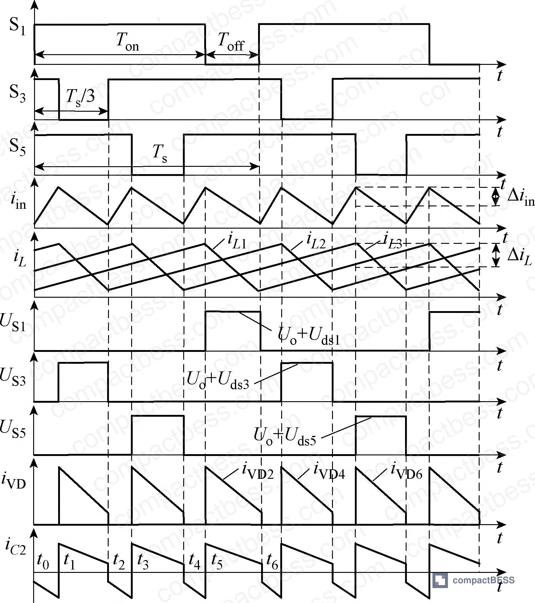
Load transient testing demonstrated that SMC-MPC maintains tighter voltage regulation during step changes. When load jumped from 18 Ω to 6 Ω (power increasing from 139 W to 417 W), output voltage dipped 2.1 V under PI-MPC control but only 1.3 V under SMC-MPC, recovering to within 1% of setpoint in 5 ms versus 13 ms. This matters for applications like vehicle jump starters and outdoor power stations where sudden motor starts or compressor engagement create step loads exceeding 300% of nominal current.
Practical Guidance for Buyers #
When qualifying suppliers for interleaved DC-DC converters, request oscilloscope captures showing all three phase currents simultaneously at low, medium, and high duty cycles. Acceptable designs show phase current deviation below 3% at any operating point, with peak-to-peak current ripple under 15% of average per-phase current. Thermal imaging during a 30-minute full-load test should reveal MOSFET case temperatures within 5°C of each other—larger deltas indicate current imbalance or inadequate thermal design.
Honestly, most buyers over-specify input voltage range and under-specify transient response. A converter that meets steady-state efficiency targets but takes 20 ms to recover from a load step will trigger nuisance BMS shutdowns in battery applications. Require suppliers to demonstrate load step response from 20% to 80% of rated power and back, capturing output voltage deviation and recovery time. This test exposes control loop bandwidth limitations that efficiency measurements miss.
For global OEM buyers working with Chinese manufacturers, CompactBESS provides technical procurement support to evaluate supplier test data and connect you with factories that can meet these current-sharing specifications. Whether you’re developing outdoor power stations or vehicle jump starters, verifying that the DC-DC stage maintains balanced phase currents under all load conditions prevents field failures and warranty claims.
Pay attention to the control architecture. Suppliers using analog control often cannot achieve the phase-by-phase duty cycle adjustment needed for tight current balance. Digital control with per-phase current sensing and independent PWM generation is non-negotiable for designs above 300 W. Ask whether the control algorithm accounts for parasitic resistance variation—if the supplier cannot explain how their controller compensates for inductor ESR mismatch, expect current imbalance issues in production units.
Need help identifying qualified suppliers for bidirectional DC-DC converters with verified current-sharing performance? Talk to our sourcing team →
Supplier Qualification Questions #
- What is the measured phase current deviation percentage across duty cycles from 0.3 to 0.7 under rated load, and can you provide oscilloscope captures showing all three phase currents simultaneously at each test point?
- What control algorithm does your DC-DC converter use to compensate for inductor parasitic resistance mismatch, and how does it adjust duty cycle independently for each phase based on measured current deviation?
- What is the output voltage overshoot percentage and settling time in milliseconds when load steps from 20% to 80% of rated power, verified by transient capture meeting IEEE 1679 recommended practice for energy storage systems characterization?
- At 500 W continuous output in boost mode with 50 V output and 20 kHz switching frequency, what is the measured input current ripple in amperes peak-to-peak and output voltage ripple in millivolts?
- During 30-minute full-load thermal testing, what is the maximum junction temperature difference in degrees Celsius between the three MOSFET channels, and does thermal imaging confirm uniform heat distribution across all power semiconductors?
Sourcing Checklist #
- [ ] Supplier provides phase current waveforms captured at three duty cycle points (0.3, 0.5, 0.7) showing deviation below 3% between any two phases
- [ ] Control architecture uses digital implementation with independent PWM generation for each phase and per-phase current sensing resolution better than 100 mA
- [ ] Load transient test data demonstrates output voltage recovery to within 1% of setpoint in under 10 ms for 20% to 80% load step per UL 9540A test method for thermal runaway section on dynamic response
- [ ] Inductor parasitic resistance values documented for all three phases with ESR variation under ±10% and inductance tolerance within ±5%
- [ ] Thermal imaging report confirms MOSFET case temperature spread below 5°C at rated power with ambient temperature 25°C and forced air cooling at specified CFM
- [ ] Input current ripple measured below 1 A peak-to-peak and output voltage ripple below 500 mV at 0.5 duty cycle, 50 V output, 12 Ω load per IEC 61960-3 portable lithium cell testing ripple limits
- [ ] Control loop bandwidth confirmed above 1 kHz by frequency response measurement showing phase margin ≥45° and gain margin ≥6 dB
- [ ] Production units include over-temperature protection triggering at junction temperature 125°C with automatic phase current rebalancing during thermal derating
Key Specifications Table #
| Parameter | Recommended Value | Verification Method |
|---|---|---|
| Phase Current Imbalance | ≤2.0% across full duty cycle range | Oscilloscope capture of all three phase currents simultaneously at 0.3, 0.5, 0.7 duty cycle with cursors measuring peak values |
| Settling Time (Load Transient) | ≤10 ms to within 1% of setpoint | Electronic load programmed for 20% to 80% step, oscilloscope capture of output voltage with 10 ms/div timebase |
| MOSFET Temperature Spread | ≤5°C between hottest and coolest channel | Thermal imaging camera scan after 30 min continuous operation at rated power, ambient 25°C |
| Input Current Ripple (Boost Mode) | ≤1 A peak-to-peak at D=0.5, 50V output | Current probe on input line, oscilloscope measurement with AC coupling and 500 ns/div timebase |
Can’t find a supplier meeting these phase current balance specifications? Submit your requirements and we’ll match you with verified manufacturers within 48 hours.
Frequently Asked Questions #
What causes phase current imbalance in three-phase interleaved converters?
Parasitic resistance mismatch between inductors (even 0.02 Ω difference), PCB trace length asymmetry, and temperature-dependent FET on-resistance variation all contribute. The phase with lowest total loop resistance draws more current, creating a positive feedback loop as that FET heats further and degrades faster.
Why does sliding mode control outperform PI control for current sharing?
Sliding mode control constructs a surface that directly incorporates current error between phases, generating phase-specific current references that compensate for parameter mismatches. PI control applies the same voltage reference to all phases and cannot distinguish which channel needs adjustment. The experimental data showed PI-MPC left 2.37% imbalance in boost mode while SMC-MPC achieved 1.98%.
How does duty cycle affect ripple in interleaved topologies?
Ripple reaches minimum when two phases overlap continuously (1/3 ≤ D ≤ 2/3), where ripple frequency triples and amplitude drops by 67%. Outside this range, single-phase conduction dominates and ripple increases. Tested units confirmed input current ripple of 0.52 A at D=0.5 compared to 1.1 A at D=0.3.
What switching frequency should I specify for 500W converters?
20 kHz balances switching loss against inductor size and ripple performance. Higher frequencies reduce passive component volume but increase FET switching loss and EMI. Lower frequencies improve efficiency but require larger inductors and generate more audible noise. The tested design used 20 kHz with 0.8 mH inductors achieving 94% efficiency.
Do I need independent current sensing for each phase?
Yes, for designs above 300 W where current imbalance directly impacts reliability. Hall-effect current sensors with 100 mA resolution per phase enable the control algorithm to measure deviation and adjust duty cycles independently. Suppliers using only input/output current sensing cannot detect or correct phase imbalance.
Published by compactbess.com Technical Team | Request a sourcing quote
Data source: Sliding Mode and Model Predictive Control for Current Sharing in Interleaved Bidirectional DC-DC Converters, Y. Yue et al., Transactions of China Electrotechnical Society, 2025


